Preparation method of in-situ porous antireflection film and preparation method of organic light-emitting diode
A technology of light-emitting diodes and anti-reflection coatings, which is applied in the manufacture of semiconductor/solid-state devices, electrical components, and electrical solid-state devices. Flexible and controllable effect in size range
- Summary
- Abstract
- Description
- Claims
- Application Information
AI Technical Summary
Problems solved by technology
Method used
Image
Examples
Embodiment 1
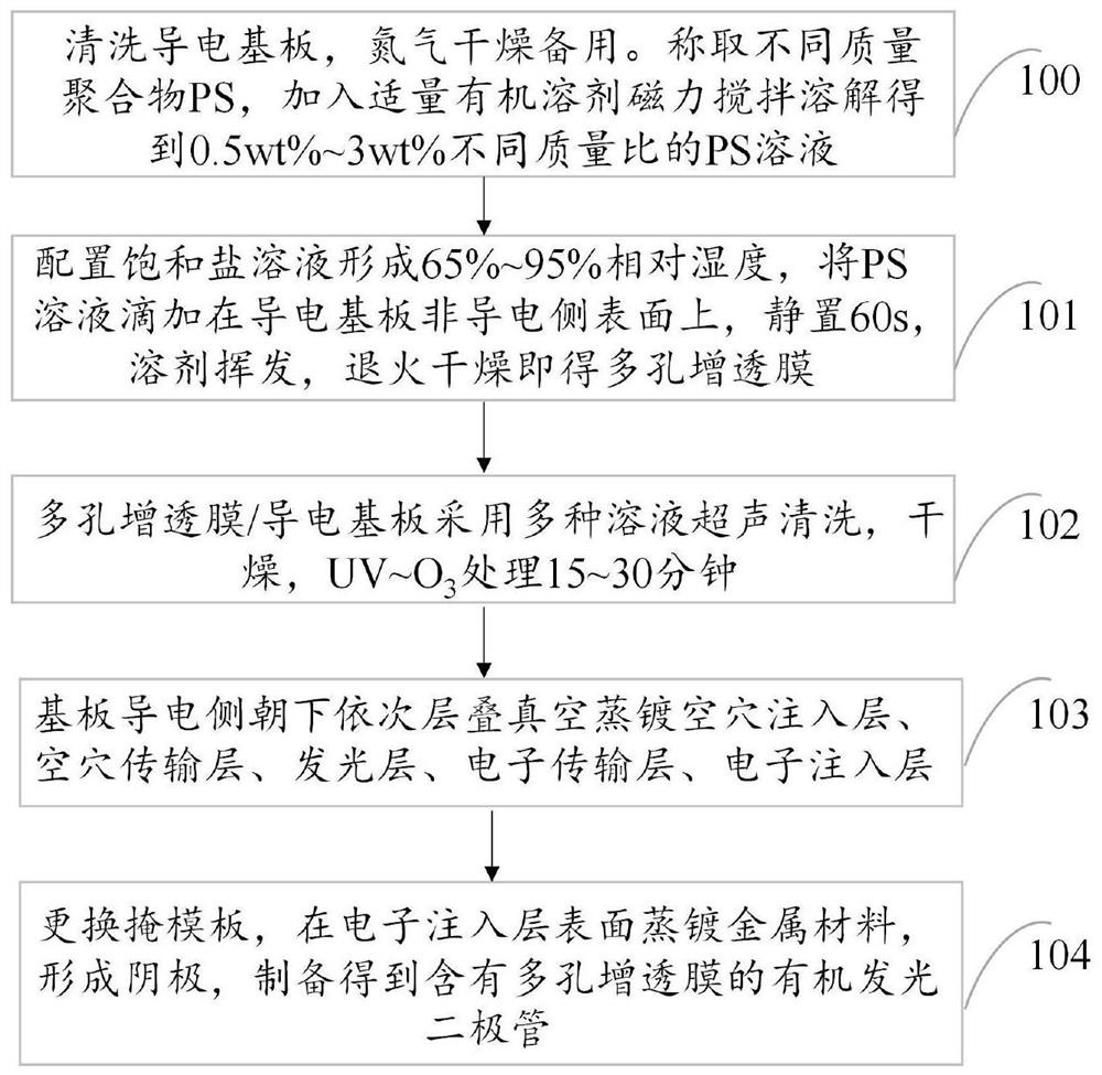
[0053] In this example, see figure 1 , a method for preparing an in-situ porous antireflection film and an organic light emitting diode, comprising the steps of:
[0054] Step 100: cleaning the ITO / glass substrate, drying with nitrogen gas for later use; weighing polymer PS of different masses, adding organic solvent chloroform to mix, stirring and dissolving by magnetic force to obtain polymer solutions with different mass ratios of 0.5wt% to 3wt%;
[0055] Step 101: configure a saturated sodium chloride solution to form a relative humidity of 75%, and after reaching a stability, add the PS solution in the step 100 dropwise on the surface of the non-conductive side of the conductive substrate after cleaning, and let it stand for 60 seconds, and the solvent will naturally volatilize; Annealed and dried to prepare a porous anti-reflection film;
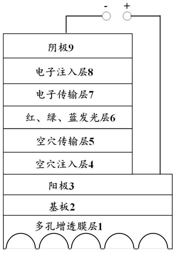
[0056] Step 102: After cleaning the dried porous membrane / ITO glass substrate in step 101 with lotion, acetone, deionized water and ...
Embodiment 2
[0062] This embodiment is basically the same as Embodiment 1, and the special features are:
[0063] In this embodiment, a method for preparing an in-situ porous anti-reflection film and an organic light-emitting diode includes the following steps:
[0064] Step 100: cleaning the ITO / glass substrate and drying it with nitrogen gas for later use. A certain mass of polymer PS was weighed, mixed with an appropriate amount of organic solvent chloroform, and dissolved by magnetic stirring to obtain a polymer PS solution with a mass ratio of 1.0 wt%.
[0065] Step 101: Configure different saturated salt solutions to form relative humidity of 65%, 75%, 85%, and 95%, and after reaching stability, add the PS solution in step 100 dropwise on the non-conductive side surface of the conductive substrate after cleaning , standing for 60s, the solvent evaporates naturally; annealing and drying can prepare a porous anti-reflection film.
[0066] Steps 102-104: this step is the same as that ...
PUM
| Property | Measurement | Unit |
|---|---|---|
| Average pore size | aaaaa | aaaaa |
Abstract
Description
Claims
Application Information


