Laser pyrolysis composite additive manufacturing integrated precursor ceramic film sensor and preparation method thereof
A technology of precursor ceramics and thin-film sensors, which is applied in the field of sensors to achieve the effects of reducing influence, increasing electrical conductivity, and good cladding and infiltration
- Summary
- Abstract
- Description
- Claims
- Application Information
AI Technical Summary
Problems solved by technology
Method used
Image
Examples
Embodiment 1
[0035] In this example, a precursor ceramic insulating group manufacturing precursor ceramic insulating base strain sensor is provided in a laser-purified composite adapter, which is sequentially insulating substrate, and the sensitive gate thickness is between 10 to 20 μm.
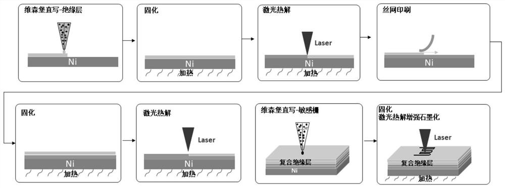
[0036] The specific preparation process of the above laser induced composite curved precursor ceramic insulating group strain sensor is like figure 1 As shown, the specifically includes the steps of:
[0037] 1) Preprocessing: First, the alumina base is easily washed 20 to 60 min, and after drying in the drying tank, take it out.
[0038] 2) Preparation of the sensitive grid: Configure the mixed solution of the conductive powder and the PDC, and use the Visen Burgon direct writing process, it is directly written to the insulating substrate of step 1), after curing for 20 minutes, laser treatment, by laser heat Solution enhancement realizes the transformation of organic material material graphitization, from A...
Embodiment 2
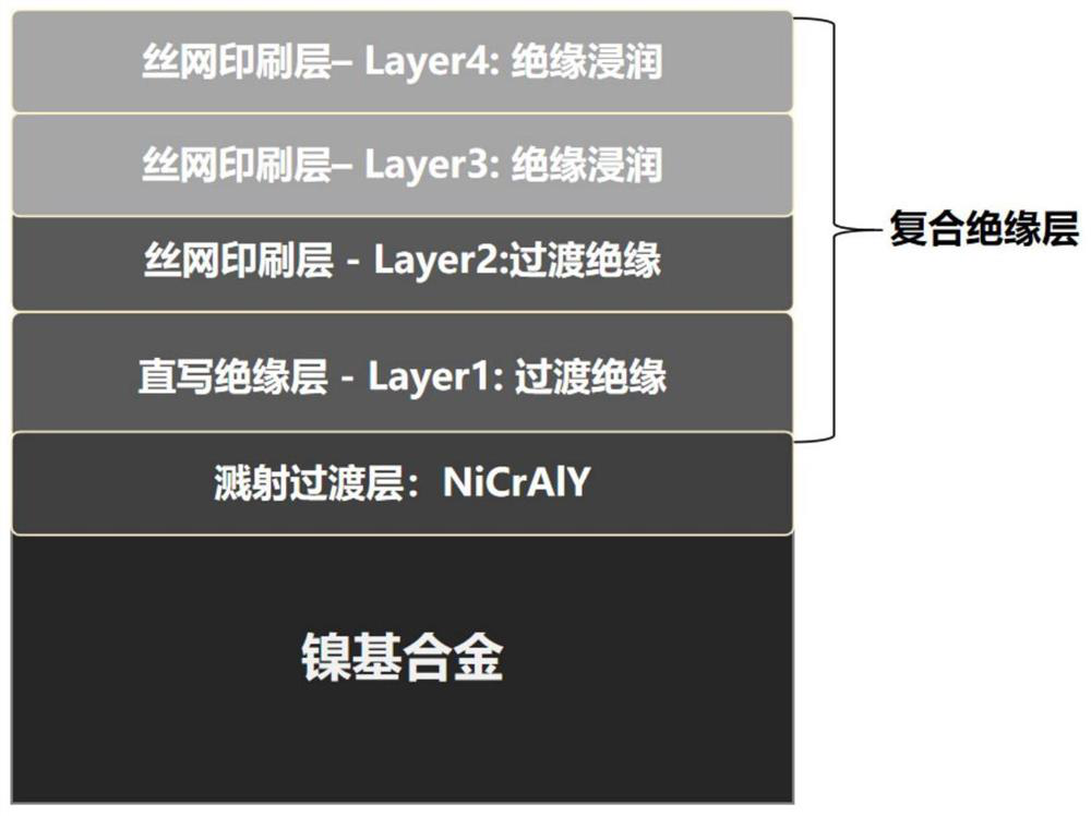
[0041]In this example, a laser-hydrolysis composite admixture manufacturing integrated precursor ceramic strain film sensor is provided, and is sequentially subjected to a nickel-based alloy substrate, a composite insulating layer, a strain-sensitive gate, wherein the composite insulating layer has a thickness of 50 to 200 μm. The sensitive gate thickness is between 10 and 20 μm.
[0042] The specific preparation process of the above precursor ceramic integrated strain sensor is like figure 2 As shown, specifically as follows:
[0043] 1) Pretreatment: The nickel-based alloy sheet is passed through an ultrasound 20 to 60 min, and after drying in the drying tank, a transition layer of 3 to 10 μm is sputtered on a nickel-based alloy sheet by a magnetron sputter.
[0044] 2) Preparation of the insulating layer: Configure the PDC solution, the insulating powder and the infiltration of the insulating powder mixed solution, and the mixture is taken out after stirring in the magnetic sti...
PUM
| Property | Measurement | Unit |
|---|---|---|
| thickness | aaaaa | aaaaa |
| thickness | aaaaa | aaaaa |
| thickness | aaaaa | aaaaa |
Abstract
Description
Claims
Application Information


