Method for preparing high-precision and large-area nano structure on insulating substrate

A nanostructure technology on an insulating substrate, applied in nanotechnology, semiconductor/solid-state device manufacturing, electrical components, etc., can solve the problems of splicing dislocation of writing field, complex operation, and not too high resolution, and achieve a large photosensitive surface , simple process and strong operability

Pending Publication Date: 2022-04-12
NANJING UNIV
View PDF4 Cites 0 Cited by
  • Summary
  • Abstract
  • Description
  • Claims
  • Application Information

AI Technical Summary

Problems solved by technology

At present, the related solutions reported include pattern correction method and exposure dose correction method. However, the actual operation of these methods is relatively complicated, and there are problems such as splicing and misalignment of writing fields in the electron beam exposure process.
In addition, there is a method to reduce the proximity effect of the electron beam by spin-coating the charge-removing gel on the sample, but the resolution of the charge-removing gel on the market is not too high (>30nm). structure doesn't help

Method used


Image

  • Method for preparing high-precision and large-area nano structure on insulating substrate
  • Method for preparing high-precision and large-area nano structure on insulating substrate
  • Method for preparing high-precision and large-area nano structure on insulating substrate

Examples


Embodiment 1

[0049] On the basis of the above method, this embodiment takes the preparation of a SNSPD with a large photosensitive surface on an insulating substrate as an example, and provides a detailed experimental operation process, including

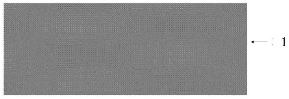
[0050] Step 1: Use acetone, ethanol and deionized water to clean the MgO insulating substrate 1 with a thickness of 500 μm. After cleaning the MgO insulating substrate 1, blow it dry with a nitrogen gun to remove the moisture on the surface of the substrate. Use AFM to measure the MgO insulating substrate 1. The surface roughness of substrate 1 RMSfigure 1 .

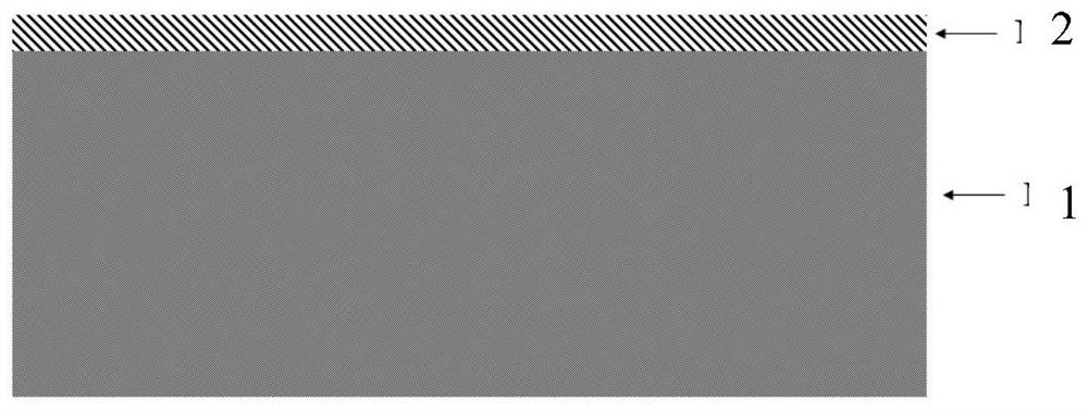
[0051] Step 2: Using a DC magnetron sputtering apparatus to grow a NbN superconducting film 2 with a thickness of 5 nm on the surface of a highly clean MgO insulating substrate 1 for preparing a micro-nano structure, the grown NbN superconducting film 2 Surface roughness RMS figure 2 For the samples shown, the samples were ultrasonically cleaned.

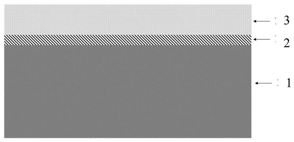
[0052] Since the NbN superconducting thi...


PUM

PropertyMeasurementUnit
thicknessaaaaaaaaaa
thicknessaaaaaaaaaa
thicknessaaaaaaaaaa

Abstract

The invention discloses a method for preparing a high-precision and large-area nano-structure on an insulating substrate, which is characterized in that one or more conductive layers are introduced between a spin-coated electron beam adhesive layer and a thin film layer to be used for preparing a micro-nano structure, so that the release rate of high-energy electrons in an electron beam exposure process is increased, a local electric field is reduced, and the stability of the nano-structure is improved. Therefore, a large amount of charges are effectively prevented from being accumulated on the surface of the insulating substrate, and a certain technical foundation is laid for further preparing a nano electronic device with a small-size, high-density and large-area micro-nano structure subsequently.

Description

technical field [0001] The invention relates to the fields of micro-nano processing technology and infrared single-photon detection technology, in particular to a method for preparing a high-precision, large-area nanostructure on an insulating substrate. Background technique [0002] Micro-nano processing technology is one of the indispensable key technologies in the process of miniaturization and large-scale integration of optoelectronic devices. At present, the minimum precision of micro-nano processing technology has been developed to below 5nm, and the performance of related equipment is also constantly improving. In scientific experiments, electron beam exposure technology is generally used to prepare micro-nano structures, and then subsequent processes such as etching are used to finally obtain the required nano-optoelectronic devices. Electron beam exposure is a key process in the development of related nanoelectronic devices. Therefore, the quality of electron beam...

Claims


Application Information

Patent Timeline
Patent Type & Authority Applications(China)
IPC IPC(8): H01L31/0352H01L21/027B82Y40/00
Inventor 张蜡宝陈奇刘梦欣李飞燕何广龙康琳吴培亨
Owner NANJING UNIV
Why Eureka
Try Eureka