A kind of Josephson junction satisfying large wafer size, preparation method and use
A wafer-sized, integrated technology, applied in the usage of superconductor elements, manufacturing/processing of superconductor devices, devices containing a node of different materials, etc., can solve the problem of increasing dielectric loss, dielectric loss, increasing loss, etc. problems, to achieve the effect of simple process steps, low dielectric loss, and high integration
- Summary
- Abstract
- Description
- Claims
- Application Information
AI Technical Summary
Problems solved by technology
Method used
Image
Examples
Embodiment 1
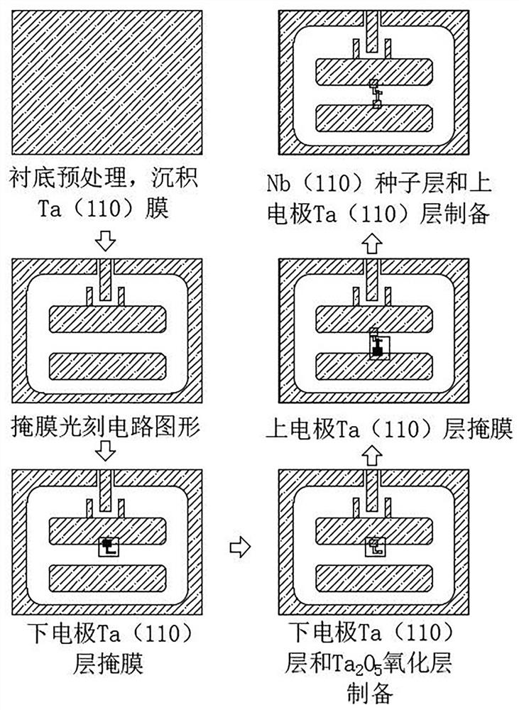
[0072] This embodiment provides a method for preparing a Josephson junction that satisfies a large wafer size. The lower electrode Ta (110) layer and the superconducting circuit pattern are formed in steps, such as figure 1 As shown, the preparation method specifically comprises the following steps:
[0073] (I) Perform surface atomic step treatment, backside pre-coating and active oxygen-assisted surface cleaning on the substrate, deposit a Ta(110) film on the C-plane sapphire substrate, and form a superconducting circuit pattern by photolithography. Prepared by magnetron sputtering method, the growth temperature is 500°C, the working pressure is 13mTorr, the DC power is 600W, the target base distance is 110mm, and the growth thickness is 100nm;
[0074] The lower electrode Ta(110) layer is prepared by mask photolithography in the overlapping area of the superconducting circuit pattern, and the lower electrode Ta(110) layer is prepared by magnetron sputtering method, includ...
Embodiment 2
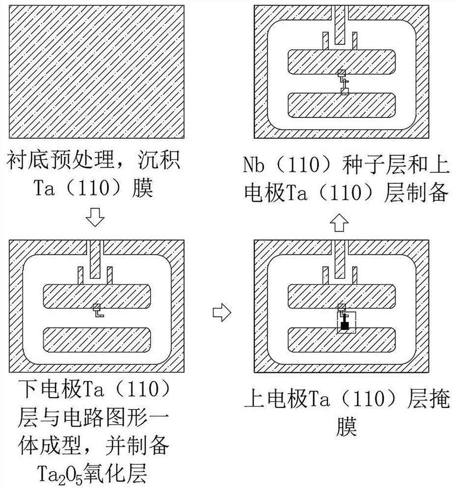
[0079] The present embodiment provides a method for preparing a Josephson junction that satisfies the size of a large wafer. The lower electrode Ta (110) layer and the superconducting circuit pattern are formed in steps, and the preparation method specifically includes the following steps:
[0080](I) Perform surface atomic step treatment, backside pre-coating and active oxygen-assisted surface cleaning on the substrate, deposit a Ta(110) film on the C-plane sapphire substrate, and form a superconducting circuit pattern by photolithography. It is prepared by magnetron sputtering method, the growth temperature is 410℃, the working pressure is 5mTorr, the DC power is 400W, the target base distance is 70mm, and the growth thickness is 50nm;
[0081] The lower electrode Ta(110) layer is prepared by mask photolithography in the overlapping area of the superconducting circuit pattern, and the lower electrode Ta(110) layer is prepared by magnetron sputtering method, including: first...
Embodiment 3
[0086] The present embodiment provides a method for preparing a Josephson junction that satisfies the size of a large wafer. The lower electrode Ta (110) layer and the superconducting circuit pattern are formed in steps, and the preparation method specifically includes the following steps:
[0087] (I) Perform surface atomic step treatment, backside pre-coating and active oxygen-assisted surface cleaning on the substrate, deposit a Ta(110) film on the C-plane sapphire substrate, and form a superconducting circuit pattern by photolithography. Prepared by magnetron sputtering method, the growth temperature is 600°C, the working pressure is 8mTorr, the DC power is 700W, the target base distance is 150mm, and the growth thickness is 150nm;
[0088] The lower electrode Ta(110) layer is prepared by mask photolithography in the overlapping area of the superconducting circuit pattern, and the lower electrode Ta(110) layer is prepared by magnetron sputtering method, including: firstly...
PUM
| Property | Measurement | Unit |
|---|---|---|
| thickness | aaaaa | aaaaa |
| thickness | aaaaa | aaaaa |
Abstract
Description
Claims
Application Information
 - R&D
- Intellectual Property
- Life Sciences
- Materials
- Tech Scout
- Unparalleled Data Quality
- Higher Quality Content
- 60% Fewer Hallucinations
Browse by: Latest US Patents, China's latest patents, Technical Efficacy Thesaurus, Application Domain, Technology Topic, Popular Technical Reports.
© 2025 PatSnap. All rights reserved.Legal|Privacy policy|Modern Slavery Act Transparency Statement|Sitemap|About US| Contact US: help@patsnap.com


