
Processing technology of anti-scratch wear-resistant 5G high-precision photoelectric integrated circuit board

A technology of optoelectronic integration and processing technology, which is applied in circuit substrate materials, printed circuit components, non-polymer adhesive additives, etc.

Pending Publication Date: 2022-05-06
江苏智纬电子科技有限公司
View PDF2 Cites 0 Cited by
  • Summary
  • Abstract
  • Description
  • Claims
  • Application Information

AI Technical Summary

Problems solved by technology

[0005] The purpose of the present invention is to provide a scratch-resistant and wear-resistant 5G high-precision optoelectronic integrated circuit board processing technology, which solves the problem that the scratch-resistant and wear-resistant effect of the integrated circuit board at the present stage is general, and the adhesive used in the circuit board has a certain degree of water absorption , so that the integrated circuit board cannot be used normally

Method used


Image

  • Processing technology of anti-scratch wear-resistant 5G high-precision photoelectric integrated circuit board
  • Processing technology of anti-scratch wear-resistant 5G high-precision photoelectric integrated circuit board
  • Processing technology of anti-scratch wear-resistant 5G high-precision photoelectric integrated circuit board

Examples


Embodiment 1

[0039] A scratch-resistant and wear-resistant 5G high-precision optoelectronic integrated circuit board processing technology, specifically including the following steps:

[0040] Step S1: Disperse the modified epoxy resin and silicon carbide in deionized water, stir at a speed of 150r / min, and a temperature of 60°C, add sodium hydroxide, react for 1h, and distill off the deionized water , to prepare glue;

[0041]Step S2: Mix alumina, silicon dioxide, calcium zirconate, potassium carbonate, and methanol, add them into a ball mill, and perform ball milling and mixing. After ball milling for 20 minutes, add adhesive liquid and modified curing agent, and continue ball milling until the mixture is uniform. The mixed material is obtained, put the mixed material into a mold, and press-molded at a temperature of 110°C to obtain a substrate, and integrate electronic components on the substrate to obtain a scratch-resistant and wear-resistant 5G high-precision optoelectronic integrate...

Embodiment 2

[0050] A scratch-resistant and wear-resistant 5G high-precision optoelectronic integrated circuit board processing technology, specifically including the following steps:

[0051] Step S1: Disperse the modified epoxy resin and silicon carbide in deionized water, stir at a speed of 180r / min and a temperature of 65°C, add sodium hydroxide, react for 1.3h, and distill to remove deionization water to make the viscous liquid;

[0052] Step S2: Mix alumina, silicon dioxide, calcium zirconate, potassium carbonate, and methanol, add them into a ball mill, and perform ball milling and mixing. After ball milling for 25 minutes, add adhesive liquid and modified curing agent, and continue ball milling until the mixture is uniform. The mixed material is obtained, put the mixed material into a mold, and press-molded at a temperature of 115°C to obtain a substrate, and integrate electronic components on the substrate to obtain a scratch-resistant and wear-resistant 5G high-precision optoelec...

Embodiment 3

[0061] A scratch-resistant and wear-resistant 5G high-precision optoelectronic integrated circuit board processing technology, specifically including the following steps:

[0062] Step S1: Disperse the modified epoxy resin and silicon carbide in deionized water, stir at a speed of 200r / min and a temperature of 70°C, add sodium hydroxide, react for 1.5h, and distill to remove deionization water to make the viscous liquid;

[0063] Step S2: Mix alumina, silicon dioxide, calcium zirconate, potassium carbonate, and methanol, add them to a ball mill, and perform ball milling and mixing. After ball milling for 30 minutes, add adhesive liquid and modified curing agent, and continue ball milling until the mixture is uniform. The mixed material is obtained, put the mixed material into a mold, and press-molded at a temperature of 120°C to obtain a substrate, and integrate electronic components on the substrate to obtain a scratch-resistant and wear-resistant 5G high-precision optoelectr...


PUM


Abstract

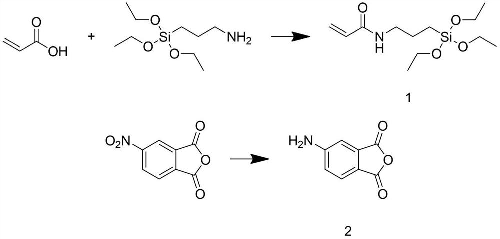
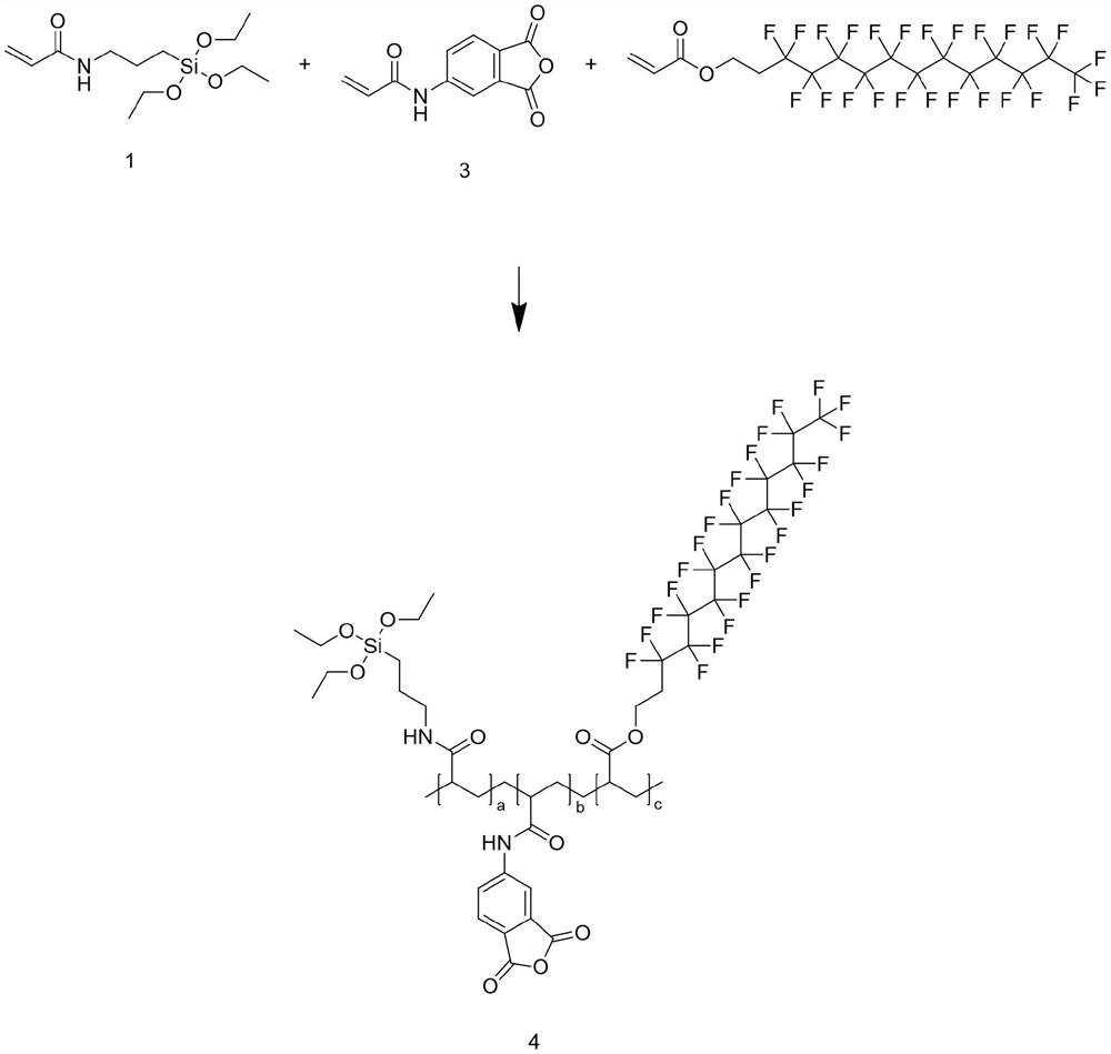
The invention discloses a processing technology of an anti-scratch wear-resistant 5G high-precision photoelectric integrated circuit board, which comprises the following steps: dispersing modified epoxy resin and silicon carbide in deionized water, stirring, adding sodium hydroxide, reacting, distilling to remove the deionized water to obtain adhesive liquid, and drying to obtain the anti-scratch wear-resistant 5G high-precision photoelectric integrated circuit board. Aluminum oxide, silicon dioxide, calcium zirconate, potassium carbonate, methyl alcohol, glue liquid and a modified curing agent are mixed and subjected to compression molding, a substrate is prepared, then electronic elements are integrated on the substrate, the integrated circuit board is prepared, a side chain of the modified epoxy resin contains long-chain fluoroalkane, the prepared integrated circuit board does not have the moisture absorption phenomenon, and the service life of the integrated circuit board is prolonged. Meanwhile, aerobic silane of a side chain is hydrolyzed to generate silanol which is grafted with active hydroxyl on the surface of the silicon carbide, so that the silicon carbide is uniformly dispersed in the adhesive liquid, the wear resistance of the adhesive liquid is improved, and the wear resistance effect of the integrated circuit board is further improved.

Description

technical field [0001] The invention relates to the technical field of integrated circuit board preparation, in particular to the processing technology of a scratch-resistant and wear-resistant 5G high-precision photoelectric integrated circuit board. Background technique [0002] Circuit substrates, according to the materials used in circuit substrates, can be divided into three categories: inorganic substrate materials, organic substrate materials and composite substrate materials. Traditional inorganic substrates are based on Al 2 o 3 , SiC, BeO and AlN as substrates, because these materials have good performance in terms of thermal conductivity, bending strength and thermal expansion coefficient, they are currently widely used in the MCM circuit substrate industry. At present, integrated circuit substrates developed at home and abroad The materials used are mainly low-temperature sintered substrate materials, which can be roughly divided into two categories, one is glas...

Claims


Application Information

Patent Timeline
IPC IPC(8): H05K1/03C09J163/00C09J11/04B29B13/10B29C43/02
CPCH05K1/03C09J163/00C09J11/04B29B13/10B29C43/02C08K3/34
Inventor 邹伟民邹嘉逸刘林
Owner 江苏智纬电子科技有限公司
Learn More