Preparation method of silicon nanospheres

A silicon nanometer and silicon wafer technology is applied in the field of preparation of silicon nanospheres, which can solve the problems of complex production process, small average particle size of silicon nanoparticle, fixed reaction area, etc., and achieves green environmental protection, large diameter, and easy operation in the preparation process. easy effect

Pending Publication Date: 2022-05-20
GUANGZHOU UNIVERSITY
View PDF7 Cites 0 Cited by
  • Summary
  • Abstract
  • Description
  • Claims
  • Application Information

AI Technical Summary

Problems solved by technology

[0005] The purpose of the present invention is to provide a method for preparing silicon nanospheres, which can solve the problems of complex production process, fixed reaction area, and small average particle size of prepared silicon nanoparticles in the current preparation method of silicon nanospheres.

Method used


Image

  • Preparation method of silicon nanospheres
  • Preparation method of silicon nanospheres
  • Preparation method of silicon nanospheres

Examples


preparation example Construction

[0036] A method for preparing silicon nanospheres, comprising the following steps:

[0037] Step 1: Ultrasonic cleaning of silicon wafers;

[0038] Step 2: Fix the cleaned silicon wafer in a quartz petri dish filled with deionized water, and fix the quartz sample cell above the three-dimensional electric translation stage of the femtosecond laser micro-nano processing system;

[0039] Step 3: Focus the femtosecond pulsed laser on the surface of the silicon wafer;

[0040] Step 4: Use the motion control software to set the movement parameters of the three-dimensional electric translation platform;

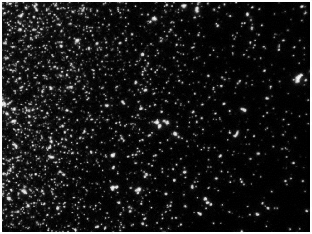
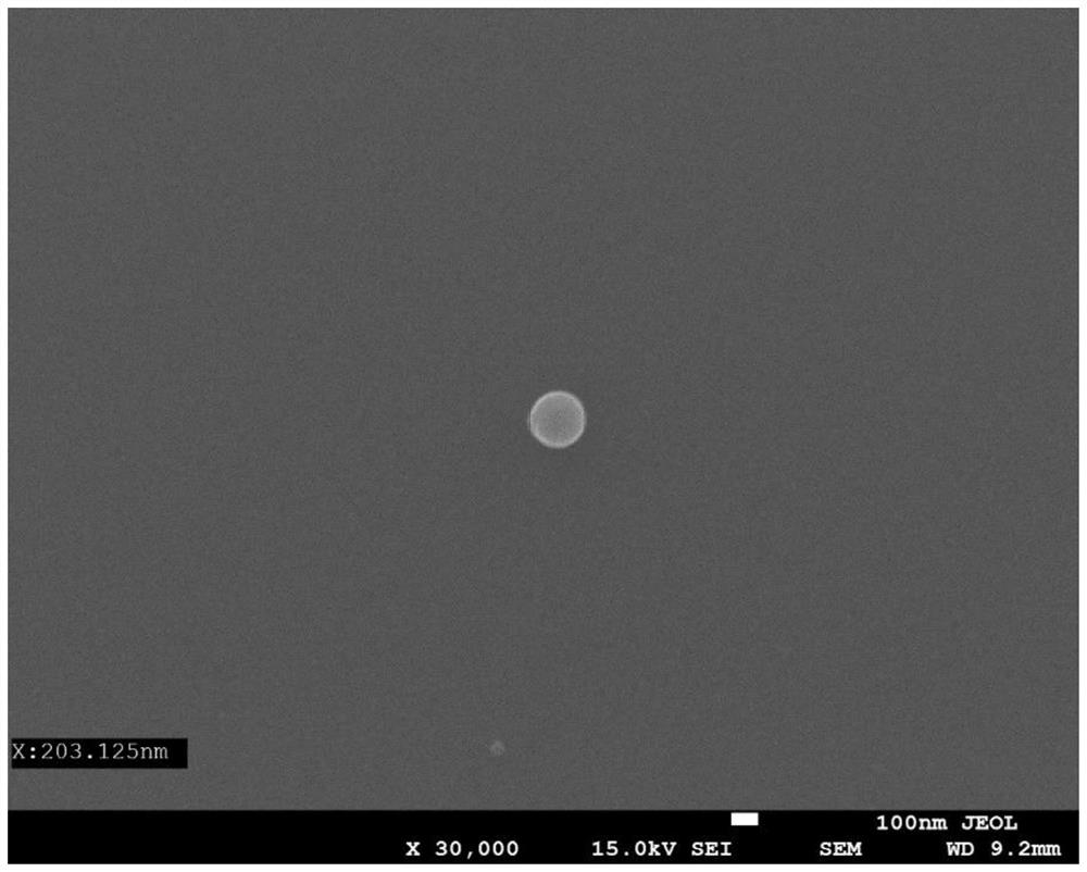
[0041] Step 5: The silicon wafer is moved by program control, and the femtosecond pulse laser ablates the surface of the silicon wafer to obtain a pale yellow colloidal silicon nano-water solution.

Embodiment 1

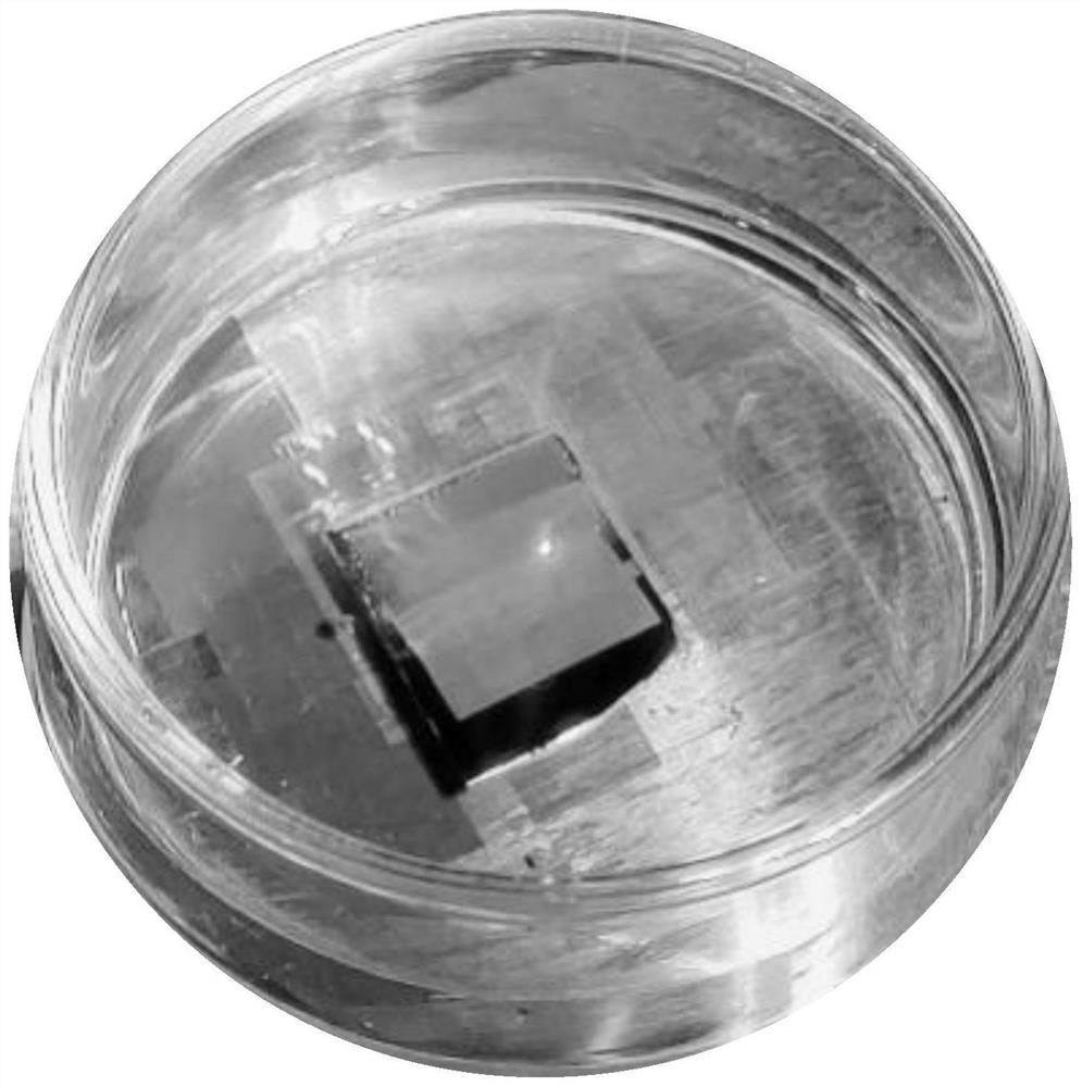
[0043] 1. The silicon wafer (10mm×12mm) and a quartz Petri dish were ultrasonically cleaned in deionized water for 20 minutes, and then dried.

[0044] 2. Fix the cleaned silicon wafer in a quartz petri dish filled with 3ml deionized water, and fix the quartz sample cell on the femtosecond laser micro-nano processing system.

[0045] 3. Lead the laser to the top of the three-dimensional electric translation platform of the femtosecond laser micro-nano processing system. The output center wavelength of the laser amplification stage used is 800nm, the pulse width is 100fs, and the repetition frequency is 1kHz. The laser power can be continuously adjusted to 4mW by combining a half-wave plate and a Glan prism. The laser is focused by a lens with a focal length of 15cm and irradiates the silicon wafer. On the surface, the diameter of the focused spot is about 40 μm.

[0046] 4. Use the motion control software to set the moving parameters of the three-dimensional electric translat...


PUM

PropertyMeasurementUnit
wavelengthaaaaaaaaaa
diameteraaaaaaaaaa
diameteraaaaaaaaaa

Abstract

The invention discloses a preparation method of silicon nanospheres. The preparation method comprises the following steps: step 1, ultrasonically cleaning a silicon wafer; 2, fixing the cleaned silicon wafer in a quartz culture dish filled with deionized water, and fixing a quartz sample pool above a three-dimensional electric translation table of a femtosecond laser micro-nano processing system; 3, focusing femtosecond pulse laser on the surface of the silicon wafer; fourthly, movement parameters of the three-dimensional electric translation table are set through movement control software; and 5, controlling the movement of the silicon wafer through a program, and ablating the surface of the silicon wafer by femtosecond pulse laser to obtain a faint yellow colloidal silicon nano aqueous solution. Compared with the prior art, the method has the characteristics of no complex process, simplicity and convenience in operation, capability of presetting parameters through software, realization of automatic preparation of the silicon nanoparticle solution and larger diameter of the prepared silicon nanospheres.

Description

technical field [0001] The invention relates to the field of preparation methods of nanomaterials, in particular to a preparation method of silicon nanospheres. Background technique [0002] Silicon nanospheres are high refractive index dielectric nanoparticles with excellent properties. Silicon nanospheres can interact strongly with light at the nanoscale, such as electric and magnetic dipole resonances, near-field magnetic field enhancement, directional scattering, and Fano resonance in the visible to near-infrared spectral range. Since silicon nanospheres have strong optical response and low material loss, they are effective materials for nanostructure optoelectronic devices such as nanoantennas. On the other hand, silicon nanospheres have good application prospects in the research direction of metasurfaces and metamaterials, especially silicon nanospheres with a characteristic size between 100 and 300 nanometers, which are excellent for the study of semiconductor metasu...

Claims


Application Information

Patent Timeline
Patent Type & Authority Applications(China)
IPC IPC(8): B23K26/0622B23K26/60C01B33/021
CPCB23K26/0624B23K26/60C01B33/021Y02E60/10
Inventor 张成云萧雪莲陈冬演郭浩民
Owner GUANGZHOU UNIVERSITY
Why Eureka
Try Eureka