

A kind of gas sensor, manufacturing method and gas detection method
A technology of gas sensor and manufacturing method, which is applied in the direction of instruments, measuring devices, scientific instruments, etc., can solve the problems of limiting the application range and application prospect of gas sensors, low response time and sensitivity of sensors, etc., and achieve shortened response time and rapid adsorption of gas Effect
- Summary
- Abstract
- Description
- Claims
- Application Information
AI Technical Summary
Problems solved by technology
Method used
Image

Examples
Embodiment 1
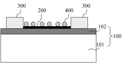
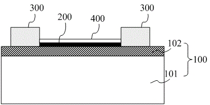
[0062] The manufacturing method of the gas sensor provided by the embodiment of the present invention includes: firstly, forming a silicon dioxide layer with a thickness of 100 nm on a silicon substrate; secondly, using a chemical vapor deposition method to form a graphene layer with a thickness of 0.34 nm on a copper substrate, and using The wet transfer method is transferred to the silicon dioxide layer, and then an inductively coupled oxygen plasma dry etching process is used to form a patterned graphene layer on the silicon dioxide layer to obtain two contact holes. Next, an electrode is formed in each contact hole, and the material of the adhesion layer is titanium with a thickness of 1 nm, and the material of the conductive layer is gold with a thickness of 50 nm. Finally, titanium dioxide nanoparticles were formed on the graphene layer by a spin coating process, where the spin coating speed was 300 r / min and the concentration of the spin coating solution was 15 g / mL.
Embodiment 2
[0064] The manufacturing method of the gas sensor provided by the embodiment of the present invention includes: firstly, forming a silicon dioxide layer with a thickness of 120 nm on a silicon substrate; secondly, using a chemical vapor deposition method to form a molybdenum disulfide layer with a thickness of 10 nm on a copper substrate; The method of etching the substrate transfers the molybdenum disulfide to the silicon dioxide layer, and then adopts the inductively coupled oxygen plasma dry etching process to form a patterned molybdenum disulfide layer on the silicon dioxide layer to obtain two contact holes . Next, an electrode is formed in each contact hole, and the material of the adhesive layer is tungsten with a thickness of 5 nm, and the material of the conductive layer is silver with a thickness of 70 nm. Finally, TiO2 nanoparticles were formed on the graphene layer by a spin-coating process, where the spin-coating speed was 700 r / min and the concentration of the sp...
Embodiment 3
[0066]The manufacturing method of the gas sensor provided by the embodiment of the present invention includes: firstly, forming a silicon dioxide layer with a thickness of 210 nm on a silicon substrate; secondly, using a chemical vapor deposition method to form a molybdenum disulfide layer with a thickness of 15 nm on a copper substrate; The method of etching the substrate transfers the molybdenum disulfide to the silicon dioxide layer, and then adopts the inductively coupled oxygen plasma dry etching process to form a patterned molybdenum disulfide layer on the silicon dioxide layer to obtain two contact holes . Next, an electrode is formed in each contact hole, the adhesion layer of which is 8 nm thick chromium, and the conductive layer material is 120 nm thick copper. Finally, TiO2 nanoparticles were formed on the graphene layer by a spin-coating process, where the spin-coating speed was 1100 r / min and the concentration of the spin-coating solution was 5 g / mL.
PUM
| Property | Measurement | Unit |
|---|---|---|
| thickness | aaaaa | aaaaa |
| thickness | aaaaa | aaaaa |
| thickness | aaaaa | aaaaa |
Abstract
Description
Claims
Application Information