A silicon carbide mosfet cell layout structure with integrated gated diode

A gate-controlled diode and layout structure technology, applied in transistors, electrical components, semiconductor devices, etc., can solve the problems of high conduction voltage drop of SiC body diodes, high JFET area density, and increased dynamic loss of devices, so as to improve long-term reliability performance, low on-resistance, increased current capability and robustness

Active Publication Date: 2022-08-05
NOVUS SEMICON CO LTD
View PDF4 Cites 0 Cited by
  • Summary
  • Abstract
  • Description
  • Claims
  • Application Information

AI Technical Summary

Problems solved by technology

[0004] However, there are two problems in the planar SiC VDMOS. One is that the density of the JFET area is relatively high, which introduces a large Miller capacitance, which increases the dynamic loss of the device; the other is that the parasitic SiC body diode conduction voltage drop is too high. , and it is a bipolar device, which has a large reverse recovery current. In addition, the bipolar degradation phenomenon caused by the silicon carbide BPD defect makes the conduction voltage drop of the body diode continue to increase with the growth of service time. Therefore, The body diode of SiC VDMOS cannot be directly used as a freewheeling diode

Method used


Image

  • A silicon carbide mosfet cell layout structure with integrated gated diode
  • A silicon carbide mosfet cell layout structure with integrated gated diode
  • A silicon carbide mosfet cell layout structure with integrated gated diode

Examples


Embodiment Construction

[0038] The following combined with the attached figures, the principle and characteristics of the present invention are described. The examples are used to explain the present invention, not to limit the scope of the present invention.

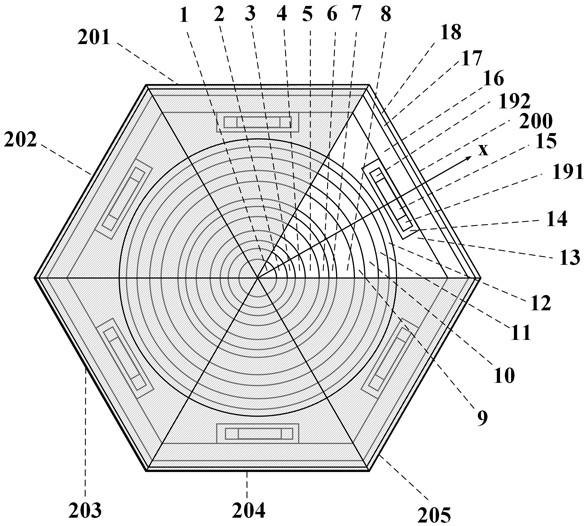
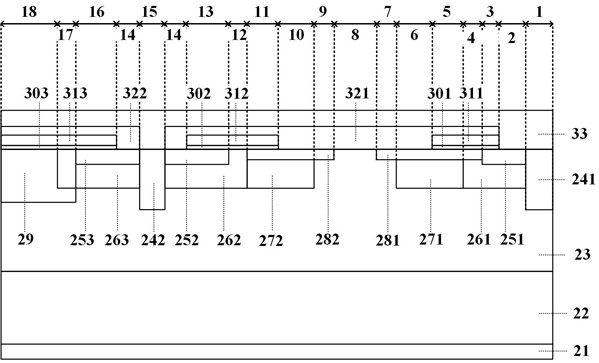
[0039] like figure 1 所示,本实施例提供一种集成栅控二极管的碳化硅MOSFET元胞版图结构,包括第一区域1,第二区域2,第三区域3,第四区域4,第五区域5,第六Area 6, Seventh Region 7, Eighth Region 8, Ninth Region 9, Tenth Region 10, Eleventh Region 11, Twelfth Region 12, 13th Region 13, 14th Area 14, Fifteenth, 15th, 15th, 15th, 15th, 15th, 15th, 15th, 15th, 15th, 15th, 15th, 15th, 15th, 15th, 15th, 15th, 15th, 15th, 15th, 15th, 15th, 15th, 15th, 15th, 15th, 15th, 15th, 15th, 15th, 15th, 15th, 15th, 15th, 15th, 15th, 15th Area 15, 16 areas 16, 17 areas 17, eighteenth area 18, 191 area 191, 192 area 192, 201 area 201, 202 area 202, No. 1, No. 1 203, 203, 204, 204, 205 areas 205.

[0040] The first area 1 is a fan of 60 degrees in the inner angle; the second region 2, the third region 3, the fourth region 4, the fi...


PUM


Abstract

The invention relates to a cell layout structure of a silicon carbide MOSFET integrated with a gate-controlled diode, and belongs to the technical field of power semiconductor devices. The invention adopts the separation gate design, and the gated diode is integrated in a single piece; the gated diode is integrated into each MOSFET cell on the layout, and the separated gate channel of the gated diode and the MOSFET is designed to be circular on the graph, In order to solve the reliability problem caused by the electric field concentration at the edge of the separation gate. In order to obtain higher channel density, the outer channel of the MOSFET is designed to be hexagonal from the layout. Compared with the method of arranging the main and auxiliary devices separately in the traditional monolithic integration, the advantage of the present invention is that the main device MOSFET and the integrated device gate-controlled diode are uniformly arranged in the whole active area, so that both devices can obtain a larger The effective heat dissipation area improves the respective current capability and robustness.

Description

Technical field [0001] The present invention is the field of power semiconductor device technology, which involves a silicon carbide MOSFET metaphysical layout method that integrates a grille control diode. Background technique [0002] Wide -and -tape semiconductor material SIC is an ideal material for preparing high -voltage electric electronic devices. Compared to SI materials, SIC materials have high intensity of breakdown electric field (4 × 10 (4 × 10 6 V / CM), high -flowing saturation drift speed (2 × 10 7 CM / S), high thermal conductivity, good thermal stability, etc., so it is especially suitable for electronic devices for high -power, high -voltage, high temperature and anti -radiation. [0003] SIC VDMOS is a more commonly used device in SIC power devices. Compared with bipolar types, because SICVDMOS does not have a charge storage effect, it has better frequency characteristics and lower switching loss. At the same time, SIC material's wide controlband makes SIC VDMOS o...

Claims


Application Information

Patent Timeline
Patent Type & Authority Patents(China)
IPC IPC(8): H01L29/06H01L29/10H01L29/739H01L29/78H01L27/02H01L27/07
CPCH01L27/0207H01L27/0716H01L29/0696H01L29/1037H01L29/1004H01L29/7827H01L29/7391
Inventor 顾航高巍戴茂州
Owner NOVUS SEMICON CO LTD
Why Eureka
Try Eureka