
Semiconductor wafer thinning device with dust treatment function

A technology for dust treatment and semiconductors, which is applied in semiconductor/solid-state device manufacturing, gas treatment, and the use of liquid separation agents, etc. It can solve the problems of easy damage to wafers, easy entry of dust into other equipment, environmental pollution, etc., and speed up the thinning rate Effect

Pending Publication Date: 2022-06-24
无锡市芯通电子科技有限公司
View PDF0 Cites 2 Cited by
  • Summary
  • Abstract
  • Description
  • Claims
  • Application Information

AI Technical Summary

Problems solved by technology

[0003] The existing wet etching thinning operation is easy to damage the front side of the wafer, and it is easy to cause environmental pollution, and the existing device does not collect and process the dust generated by thinning, and the dust is easy to enter other equipment and affect the operation of other equipment. service life and is detrimental to the health work needs of the operator

Method used


Image

  • Semiconductor wafer thinning device with dust treatment function
  • Semiconductor wafer thinning device with dust treatment function
  • Semiconductor wafer thinning device with dust treatment function

Examples


Embodiment 1

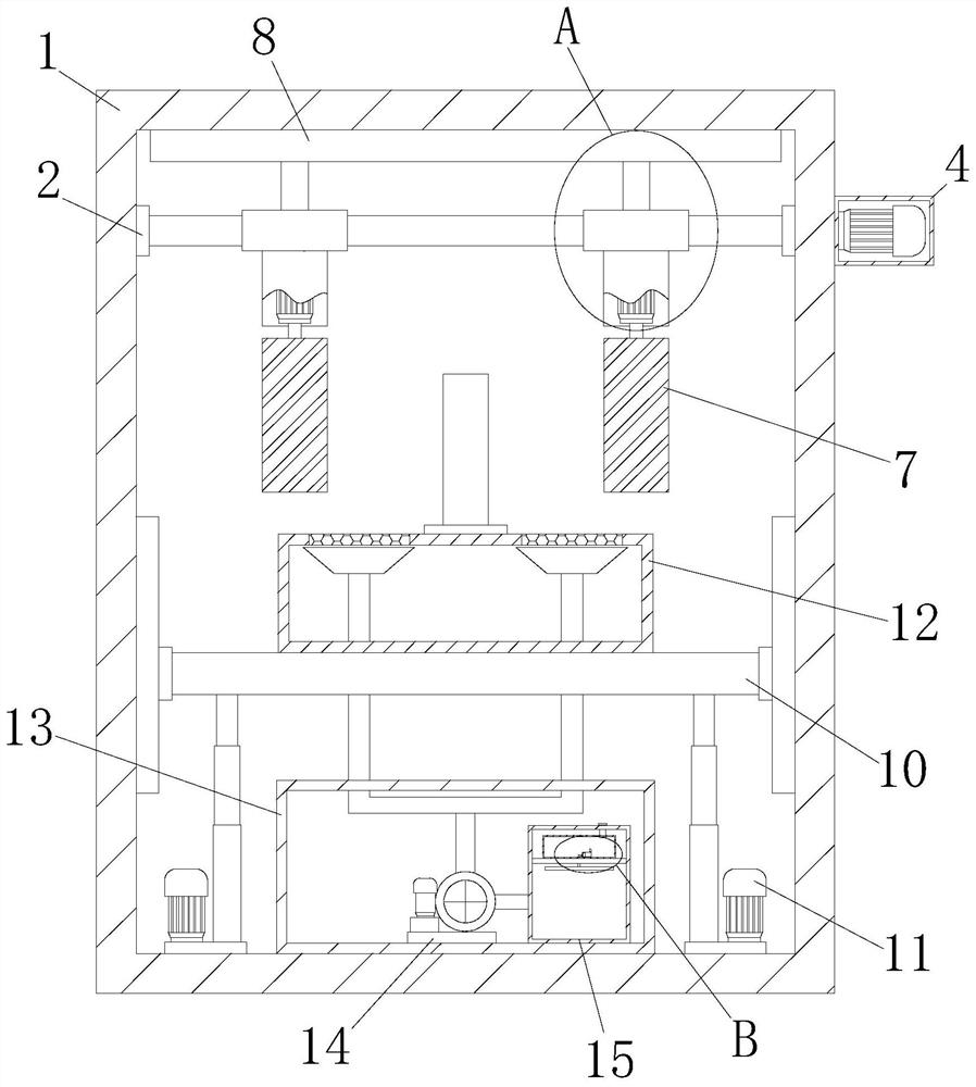
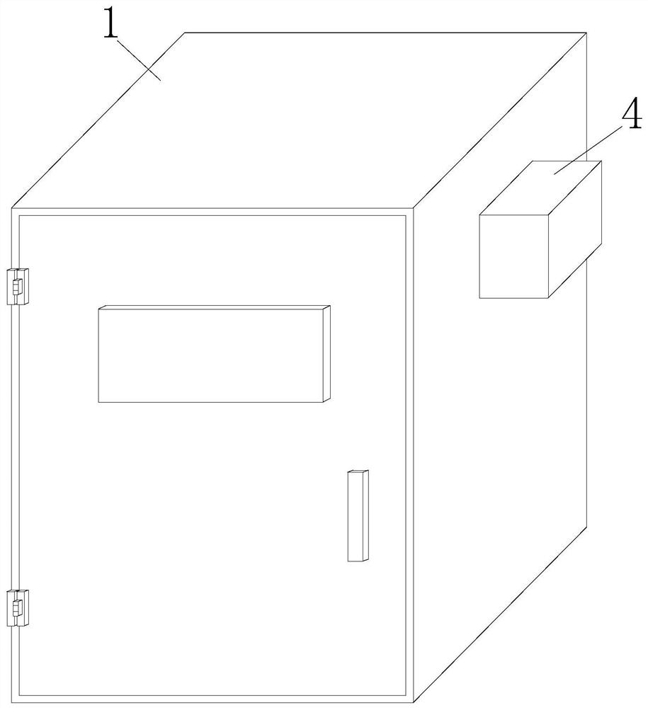
[0023] according to Figure 1-4 , a semiconductor wafer thinning device with a dust processing function, comprising a thinning box 1 , a thinning mechanism and a collecting mechanism, both of which are fixedly installed in the thinning box 1 .

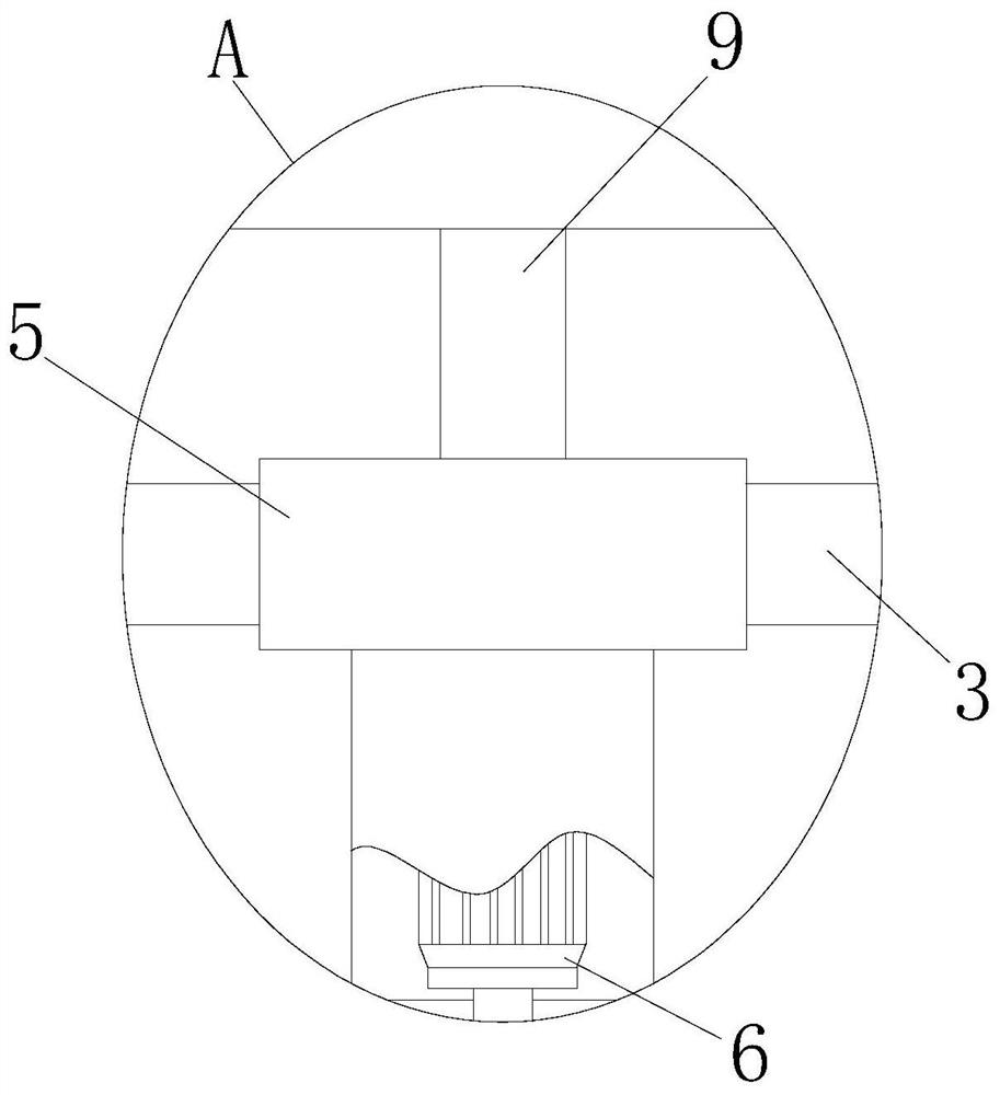
[0024] The thinning mechanism includes a threaded rod 3, a threaded barrel 5, a thinning motor 6, a carrier plate 10 and a multi-stage electric push rod 11. A threaded rod 3 is rotatably installed between the two side plates corresponding to the thinning box 1, and the threaded rod 3 Two threaded barrels 5 are threadedly connected to the outer wall of the thinning box 1, a first slide rail 8 is fixedly installed on the bottom surface of the top plate of the thinning box 1, and two first slide blocks 9 are slidably installed inside the first slide rail 8. The bottoms of the blocks 9 are respectively fixedly connected to the tops of the corresponding threaded cylinders 5, the bottoms of the two threaded cylinders 5 are fixedly installed ...

Embodiment 2

[0030] according to Figure 1-4 , a semiconductor wafer thinning device with a dust processing function, comprising a thinning box 1 , a thinning mechanism and a collecting mechanism, both of which are fixedly installed in the thinning box 1 .

[0031] The collection mechanism includes a processing box 13, a fan 14, a storage box 15 and a micro water pump 17. The processing box 13 is fixedly installed on the top surface of the bottom plate of the thinning box 1, and a fan 14 is fixedly installed inside the processing box 13. In the storage block 12, the air outlet end of the fan 14 is movably sleeved in the storage box 15, the storage box 15 is fixedly installed with a water storage box 16, and the top surface of the bottom plate of the water storage box 16 is fixedly installed with a micro water pump 17, and the micro water pump 17 The water outlet pipe runs through the bottom plate of the water storage box 16 and is fixedly sleeved with an atomizing nozzle 18 .

[0032] Whi...


PUM


Abstract

The invention relates to the technical field of wafer processing, in particular to a semiconductor wafer thinning device with a dust treatment function. The invention aims to solve the technical problems that wafers are easy to damage and dust is not collected. In order to solve the technical problem, the semiconductor wafer thinning device with the dust treatment function is mainly composed of a thinning mechanism and a collecting mechanism, through arrangement of a threaded cylinder, a thinning roller and a multi-stage electric push rod, silicon wafers can be continuously polished, the thinning rate of the wafers is increased, and the efficiency of the wafers is improved. The distance between the two thinning rollers can be adjusted according to the thinning size requirement, the thinning requirements of different sizes can be met, dust generated by thinning can be collected and treated while the thinning operation is carried out by arranging a fan and a storage box, and through a water storage box, a micro water pump and an atomization spray head, the dust can be effectively prevented from being corroded by the water storage box, the micro water pump and the atomization spray head. And the collected dust is subjected to rapid dust falling treatment.

Description

technical field [0001] The invention relates to the technical field of wafer processing, in particular to a semiconductor wafer thinning device with a dust processing function. Background technique [0002] Wafer refers to the silicon wafer used to make silicon semiconductor circuits. Its original material is silicon. The wafer needs to undergo a series of processing before it is finally used. In order to meet various needs, the thinning of the wafer is a part of its processing. One of the important links of the wafer thinning technology, the existing wafer thinning technologies mainly include: grinding, chemical mechanical polishing, wet etching, atmospheric pressure plasma etching, etc. The principle of wet etching is to immerse the wafer in a chemical solution, through chemical reaction Removal of wafer surface material but existing semiconductor wafer thinning devices have many problems or defects; [0003] The existing wet etching thinning operation is easy to damage t...

Claims


Application Information

Patent Timeline
Patent Type & Authority Applications(China)
IPC IPC(8): H01L21/67B01D47/06
CPCH01L21/67092H01L21/67017B01D47/06B01D2258/0216
Inventor 葛光华吴浩栋曾兰英罗江萍刘磊
Owner 无锡市芯通电子科技有限公司
Learn More