Transparent perovskite thin film transistor

A thin film transistor and perovskite technology, which is applied in the field of preparation of transparent perovskite thin film transistors, can solve the problems of difficulty in preparing transparent perovskite thin film transistors, inability to prepare single crystal devices in a large area, and limited application value. Achieve the effect of improving electron injection efficiency, simple substrate processing method, and good application potential

Pending Publication Date: 2022-07-05
HUNAN UNIV
View PDF1 Cites 0 Cited by
  • Summary
  • Abstract
  • Description
  • Claims
  • Application Information

AI Technical Summary

Problems solved by technology

However, due to the ion-shielding effect of perovskite materials, it is difficult for transistors fabricated by common thin-film transistor fabrication methods to work effectively at room temperature.
In addition, for transparent perovskite films such as MAPbCl 3 thin film, its band gap is wide, and the gold-semi-contact barrier is large, so that electrons cannot be effectively injected into MAPbCl 3 Therefore, it is difficult to prepare transparent perovskite thin film t

Method used


Image

  • Transparent perovskite thin film transistor
  • Transparent perovskite thin film transistor
  • Transparent perovskite thin film transistor

Examples


Embodiment 1

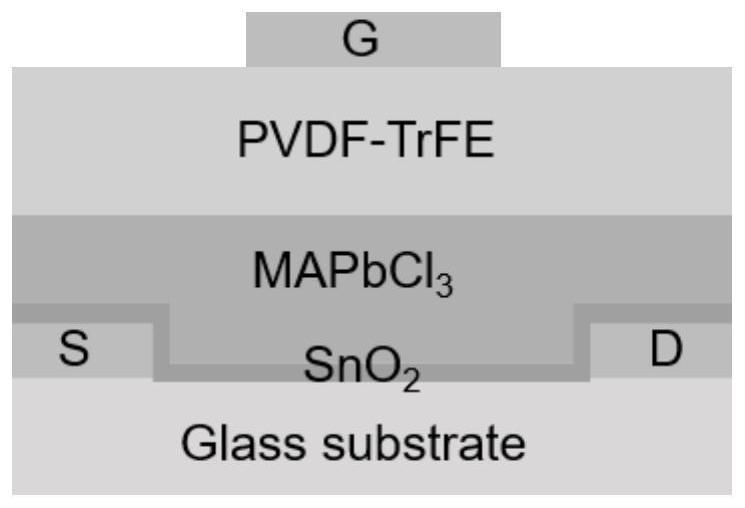
[0022] In this embodiment, a top-gate bottom-contact transistor is used as an example, and other bottom-gate top-contact, top-gate top-contact, and top-gate-bottom contact can be made into corresponding transistors only by changing the positions of the corresponding electrodes.

[0023] see figure 1 , a transparent perovskite thin film transistor includes a transparent substrate (glass), a source electrode (Cr), a drain electrode (Cr), a gate electrode (Al), an insertion layer (SnO 2 ), semiconductor layer (MAPbCl 3 ), a ferroelectric dielectric layer (PVDF-TrFE); the thickness of the insertion layer is 10 nm, and the thickness of the ferroelectric dielectric layer is 400 nm.

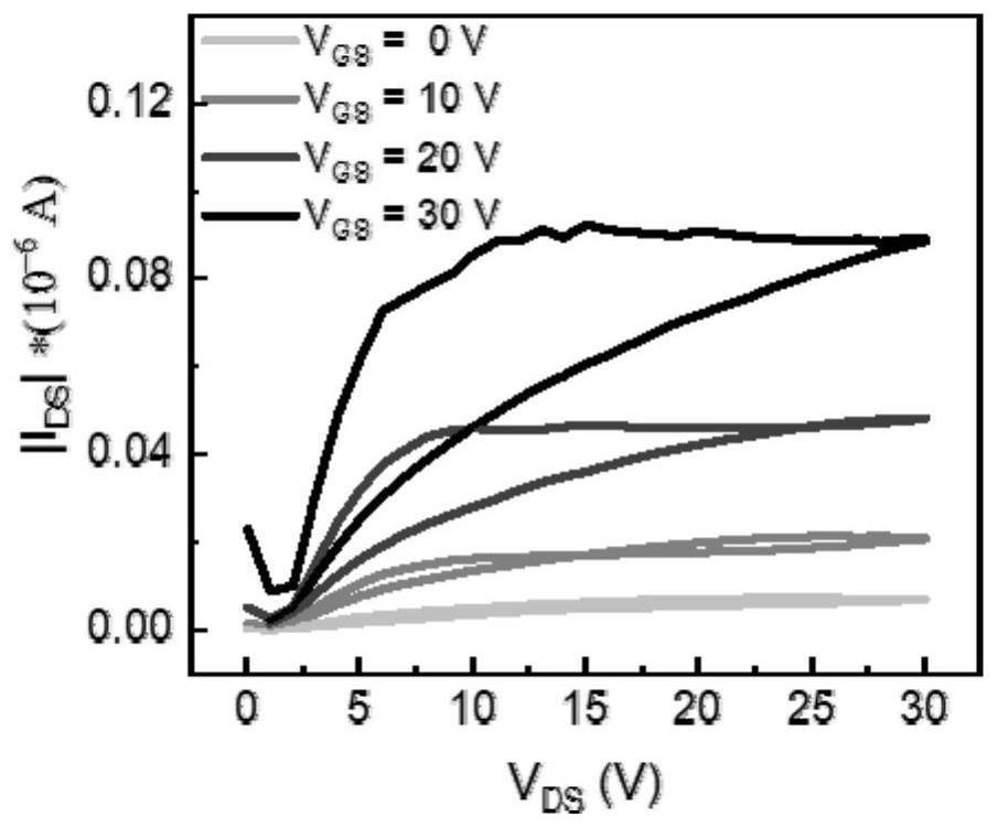
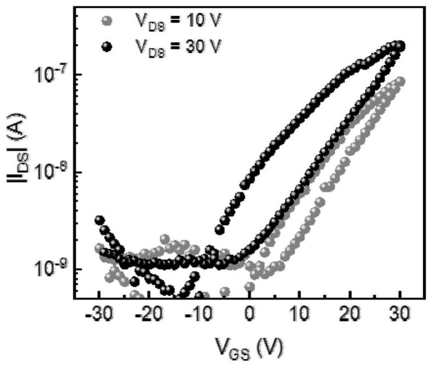
[0024] For transparent MAPbCl 3 Thin film transistor electrical testing, showing transistor output and transfer characteristics at room temperature, as shown in the appendix Figure 2-3 As shown, it can be seen from the transfer characteristic curve and the output characteristic curve that the transi...

Embodiment 2

[0026] Correspondingly, the present embodiment provides a method for preparing a transparent perovskite thin film transistor with a top-gate bottom-contact electrode. The method generally includes the following steps: using MAC1 and PbAc 2 It is a perovskite precursor liquid material, and PVDF-TrFE is a dielectric layer material to prepare a transparent perovskite thin film transistor. The specific steps are as follows:

[0027] Step 1: Process a transparent substrate with photolithographic electrodes; select a glass sheet with chrome-gold electrodes as the substrate. First, the glass slides were cleaned, followed by ultrasonic cleaning with deionized water, acetone and isopropanol for 1 min, and dried with an argon gun after cleaning. Then the glass sheet was transferred to an ozone treatment device for 15 min to change the wettability of the surface of the glass sheet.

[0028] Step 2: spin-coating the metal oxide solution, annealing at low temperature to form the intercala...


PUM

PropertyMeasurementUnit
Thicknessaaaaaaaaaa
Thicknessaaaaaaaaaa
Thicknessaaaaaaaaaa

Abstract

The transparent perovskite thin film transistor comprises a transparent substrate, a source electrode, a drain electrode, a gate electrode, an insertion layer, a semiconductor layer and a ferroelectric dielectric layer, the insertion layer is a transparent metal oxide and is arranged between the source electrode, the drain electrode and the semiconductor layer; the ferroelectric dielectric layer is located between the gate electrode and the semiconductor layer; the semiconductor layer is a transparent perovskite thin film. A layer of metal oxide thin film is inserted between the source electrode, the drain electrode and the transparent perovskite thin film to serve as an electron injection layer so as to reduce the electron injection barrier and improve the electron injection efficiency. Meanwhile, a ferroelectric material is used as a dielectric layer to inhibit a gate voltage shielding effect caused by ion migration of the transparent perovskite thin film; the transparent perovskite thin film transistor prepared on the basis can work at room temperature and is good in stability.

Description

technical field [0001] The invention belongs to the field of organic-inorganic hybrid perovskite organic field effect transistors, and more particularly, relates to the preparation of transparent perovskite thin film transistors. Background technique [0002] In recent years, organic-inorganic hybrid perovskites have attracted extensive attention as solution-processable semiconductor materials. First-principles theoretical calculations show that organic-inorganic hybrid perovskites exhibit bulk mobilities as high as 10–100 cm 2 V -1 S -1 . Its high carrier mobility and long carrier diffusion length make it have good optical and electrical properties. At the same time, the high absorption coefficient, tunable band gap, and low temperature solution processing characteristics of this material make it have broad application prospects in the field of optoelectronic devices. [0003] MAPbCl 3 It is a typical organic-inorganic hybrid perovskite, which has a wide band gap (2.9...

Claims


Application Information

Patent Timeline
IPC IPC(8): H01L51/05H01L51/10
CPCH10K10/468H10K10/462H10K10/471H10K10/82
Inventor 胡袁源夏江南仇鑫灿
Owner HUNAN UNIV
Why Eureka
Try Eureka