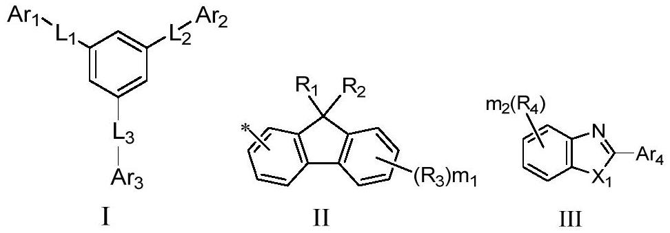
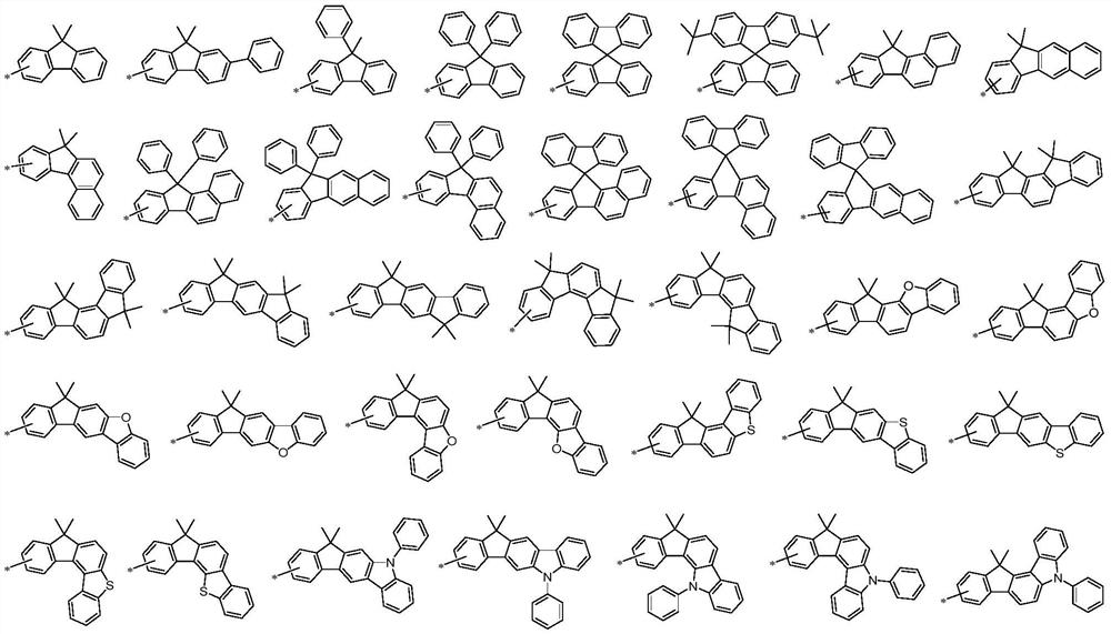
Electron injection layer material and organic electroluminescent device
A technology for electroluminescent devices and electron injection layers, which is applied in the direction of organic semiconductor devices, electric solid devices, electrical components, etc., can solve the problems of affecting electron injection capabilities, active chemical properties, and difficult storage, so as to improve luminous performance and reduce Electron injection barrier, effect of improving balance
- Summary
- Abstract
- Description
- Claims
- Application Information
AI Technical Summary
Problems solved by technology
Method used
Image
Examples
preparation example Construction
[0038] The preparation of the organic electroluminescent device of the present invention adopts a vacuum evaporation system, and the preparation is completed by continuous evaporation under the condition of uninterrupted vacuum. The materials used are in different evaporation source quartz crucibles, and the temperature of the evaporation source can be controlled separately.
[0039] The anode of the organic electroluminescent device of the present invention can use a material with a large work function, for example: metals such as vanadium, chromium, copper, zinc, gold or alloys thereof; metal oxides such as zinc oxide, indium oxide, indium oxide Tin (indium tin oxide, ITO) and indium zinc oxide (indium zinc oxide, IZO); combinations of metals and oxides, such as ZnO:Al or SnO 2 : Sb; conductive polymers, such as poly(3-methyl compound), poly[3,4-(ethylene-1,2-dioxy) compound] (PEDOT), polypyrrole and polyaniline, etc., but not limited to this.
[0040] The negative electro...
Embodiment 1
[0084] Clean the ITO glass substrate twice in distilled water, ultrasonically wash for 30 minutes, after distilled water cleaning, isopropanol, acetone, methanol and other solvents are sequentially ultrasonically washed and then dried, transferred to a plasma cleaner, and the above substrate is washed 5 minutes, sent to the evaporation machine. Evaporate hole injection layer HAT-CN / 15nm layer by layer, hole transport layer NPB / 120nm, light-emitting layer as the main body BH: doped with 10% BD / 20nm, hole blocking layer of the present invention compound 17 / 5nm, electron transport layer Alq 3 / 25nm, electron injection layer Li 2 CO 3 : Doped with 2% Yb / 2nm, cathode Al / 300nm.
[0085]
Embodiment 2
[0087] Clean the ITO glass substrate twice in distilled water, ultrasonically wash for 30 minutes, after distilled water cleaning, isopropanol, acetone, methanol and other solvents are sequentially ultrasonically washed and then dried, transferred to a plasma cleaner, and the above substrate is washed 5 minutes, sent to the evaporation machine. Evaporate hole injection layer HAT-CN / 15nm layer by layer, hole transport layer NPB / 120nm, light-emitting layer as the main body BH: doped with 10% BD / 20nm, hole blocking layer of the present invention compound 82 / 5nm, electron transport layer Alq 3 / 25nm, electron injection layer Li 2 CO 3 : Doped with 5% Yb / 2.5nm, cathode Al / 300nm.
PUM
| Property | Measurement | Unit |
|---|---|---|
| Thickness | aaaaa | aaaaa |
| Thickness | aaaaa | aaaaa |
Abstract
Description
Claims
Application Information


