Exposed welding leg of chip packaging body and processing method of exposed welding leg

A technology of chip packaging and processing methods, which is applied in the manufacture of semiconductor devices, electrical solid devices, semiconductor/solid devices, etc., can solve the problems of not being able to observe solder piles, tin out observations are not obvious, and connections are not in conformity, etc., so as to facilitate observation , to avoid oxidation, to avoid the effect of virtual welding

Active Publication Date: 2022-07-22
HEFEI SMAT TECH CO LTD
View PDF6 Cites 3 Cited by
  • Summary
  • Abstract
  • Description
  • Claims
  • Application Information

AI Technical Summary

Problems solved by technology

[0003] When the chip package is soldered to the soldering board, the soldering quality has a profound impact, and the failure caused by poor semiconductor soldering has attracted more and more attention, because this failure is often fatal and irreversible, so in semiconductor packaging technology , After the package is welded on the PCB with solder, it is necessary to use a microscope to check whether the connection between the package and the PCB meets the requirements. If there is solder accumulation at one end, it means that the solder between the PCB board and the solder pins of the package is sufficient. If there is no solder accumulation at the end of the package solder pins, it means that the solder between the PCB board and the solder pins of the package is insufficient, and the connection between the two is not good. meet the requirements
[0004] When our package is formed, the solder feet are exposed on the outer surface of the package and the height is low, and there is a certain distance from the side edge of the package, such as figure 1 As shown, when the package is soldered on the PCB, tin solder is applied to both the solder feet and the PCB board, and then the solder feet are attached to the corresponding area of ​​the PCB board. The material of the solder feet is generally copper, and the solder will not climb. For bare copper, even if the surface of the solder pins is plated with a layer of tin during the production process, due to the low height of the solder pins of our company, there is a certain distance from the side edge of the package, and the tin climbing effect may occur, but it is difficult to observe , the observation of tin out is not obvious, and the solder pile cannot be observed from the side of the package with solder feet, which is prone to the problem of virtual soldering

Method used


Image

  • Exposed welding leg of chip packaging body and processing method of exposed welding leg
  • Exposed welding leg of chip packaging body and processing method of exposed welding leg
  • Exposed welding leg of chip packaging body and processing method of exposed welding leg

Examples


Embodiment Construction

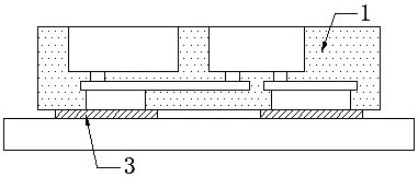
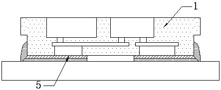
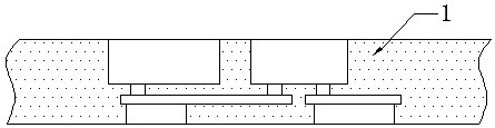
[0029] The directional terms mentioned in the present invention, such as: up, down, left, right, front, rear, inside, outside, front, back, side, etc., are only the directions with reference to the accompanying drawings, and the following implementations are described with reference to the accompanying drawings. The manners and the directional terms used are exemplary and are only used to explain the present invention and should not be construed as limiting the present invention. In addition, various specific process and material examples are provided herein, and those of ordinary skill in the art will recognize the application of other processes and / or the use of other materials.

[0030] In order to better understand the purpose, structure and function of the present invention, the following is in conjunction with the appendix Figure 1-8 , a chip package body exposed solder fillet and its processing method proposed by the present invention will be further described in detai...


PUM


Abstract

The invention discloses a chip packaging body exposed welding pin and a processing method thereof, and belongs to the technical field of semiconductor packaging, and the processing method comprises the following steps: after a packaging body is formed, forming a protruding welding pin on the packaging body before the packaging body is cut, so as to replace the step of forming the welding pin while forming a conductive layer group on the packaging body. Firstly, a plurality of cutting grooves are formed in a packaging body, each cutting groove is formed in the position of a cutting channel to be cut on the packaging body, each cutting groove is divided into two parts which are symmetrical left and right by the cutting channel, protruding weld legs are formed on the packaging body and in the cutting grooves, and the protruding weld legs comprise side weld legs and bottom weld legs. According to the packaging body, an original plate-shaped welding leg is changed into the L-shaped protruding welding leg wrapping the right-angle side of the packaging body, the forming sequence of the welding leg is changed, machining is convenient, tin climbing is obvious when the packaging body is welded, observation is convenient, and pseudo soldering is avoided.

Description

technical field [0001] The invention belongs to the technical field of semiconductor packaging, and in particular relates to a chip package body exposed solder feet and a processing method thereof. Background technique [0002] An integrated circuit is a miniature electronic device or component that uses appropriate processes such as photolithography, epitaxy, diffusion, physical vapor deposition, chemical vapor deposition, wire bonding, flip-chip, etc. to combine transistors, resistors, capacitors required in a circuit Together with components such as inductors and wiring interconnections, it is fabricated on a small or several small semiconductor wafers or dielectric substrates, and then packaged in a package to become a microstructure with the required circuit functions, that is, a semiconductor package or chip. , Semiconductor packaging refers to the process of processing the tested wafers to obtain independent chips according to the product model and functional requirem...

Claims


Application Information

Patent Timeline
Patent Type & Authority Applications(China)
IPC IPC(8): H01L21/50H01L21/56H01L21/60H01L23/31H01L23/488
CPCH01L21/50H01L21/568H01L23/488H01L23/3107H01L2021/60007H01L2924/18161
Inventor 张光耀
Owner HEFEI SMAT TECH CO LTD
Why Eureka
Try Eureka