Volatile organic pollutant detector and preparation method thereof
A volatile organic and pollutant technology, applied in the direction of material resistance, can solve the problems of harsh working environment, high working temperature, low sensitivity, etc., and achieve the effect of improving sensitivity, improving characterization ability, and high sensitivity
- Summary
- Abstract
- Description
- Claims
- Application Information
AI Technical Summary
Problems solved by technology
Method used
Image
Examples
preparation example Construction
[0047] Please refer to figure 2 , a preparation method of a detector for detecting volatile organic pollutants, comprising the steps of:
[0048] Site-directed defect modification of the sensing material and doping of a mixture of tetramethylammonium hydroxide and polydimethylglutarimide;
[0049] Fabrication of field effect transistors based on defect-modified and doped sensing materials;
[0050] The detector for detecting volatile organic pollutants is prepared according to the field effect transistor.
[0051] It can be seen from the above description that the sensing material obtained by doping the sensing material with a mixture of tetramethylammonium hydroxide and polydimethylglutarimide after the fixed-point defect modification is used to prepare a field effect transistor can improve the volatilization rate. Sensitivity of an organic pollutant detector at a lower cost and simpler procedures.
[0052] Further, the preparation of the field effect transistor includes: ...
Embodiment 1
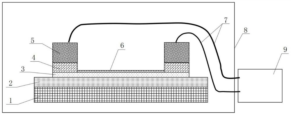
[0076] Please refer to figure 1 , a volatile organic pollutant detector, comprising an electrical signal conductor 8 and an electrical signal analyzer 9; the electrical signal conductor 8 is a field effect transistor type electrical signal conductor 8;
[0077] the field effect transistor includes an inductive material;
[0078] The sensing material is subjected to site-specific defect modification and doping of a mixture of Tetramethy1ammoniumhydroxide13 and Polydimethylglutarimide;
[0079] Wherein, the field effect transistor includes an inductive material layer, an active site layer 6 and an electrode region doping layer 4; the inductive material layer includes an inductive material.
[0080] The sensing material is a single-layer two-dimensional material, and the single-layer two-dimensional material may be two-dimensional materials such as molybdenum disulfide, boron nitride, graphene, graphene oxide, gallium arsenide, and gallium nitride. The single-layer two-dimensio...
Embodiment 2
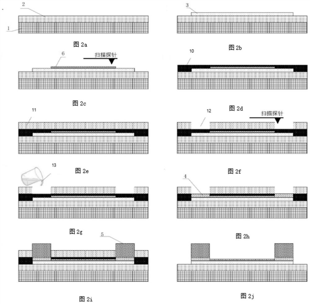
[0093] Please refer to figure 2 , a preparation method of a detector for detecting volatile organic pollutants, comprising the steps of:
[0094] S1, performing fixed-point defect modification on the sensing material and doping of a mixture of tetramethylammonium hydroxide 13 and polydimethylglutarimide 10;
[0095] Specifically, silicon with a thickness of 500 microns is selected as the gate substrate 1;
[0096] S101, oxidizing the gate substrate 1 so that a silicon dioxide gate oxide layer 2 is grown on the surface, such as figure 2 as shown in a;
[0097] Wherein, the thickness of the gate oxide layer 2 is 185 nanometers, and the optical reflection contrast of the single-layer two-dimensional material under this thickness is the highest, which is beneficial to the subsequent transfer and positioning of the two-dimensional material;
[0098] S102, transfer the molybdenum disulfide layer 3 as the sensing material on the side of the gate oxide layer 2 away from the gate ...
PUM
| Property | Measurement | Unit |
|---|---|---|
| size | aaaaa | aaaaa |
| thickness | aaaaa | aaaaa |
| thickness | aaaaa | aaaaa |
Abstract
Description
Claims
Application Information


