
EDA algorithm, application and simulation method for P-type GaN quantum well device transport characteristics

A simulation method and quantum well technology, which are applied in quantum computers, complex mathematical operations, design optimization/simulation, etc., can solve problems such as the inability to accurately describe the internal mechanism, the coupling effect of complex energy bands, and the inability to describe the structure of valence band quantum wells, etc. Achieve the effect of low cost, promotion of application, and convenience and compatibility

Pending Publication Date: 2022-07-29
SYNERGY INNOVATION INST OF GDUT HEYUAN
View PDF0 Cites 0 Cited by
  • Summary
  • Abstract
  • Description
  • Claims
  • Application Information

AI Technical Summary

Problems solved by technology

Due to the strong anisotropic nature of the quantum well structure at the GaN / AlN heterojunction interface and the complex energy band coupling effect, the general bulk material analysis method and TCAD software cannot accurately describe its internal mechanism and carry out Accurate simulation, there is a problem that the valence band quantum well structure cannot be accurately described

Method used


Image

  • EDA algorithm, application and simulation method for P-type GaN quantum well device transport characteristics
  • EDA algorithm, application and simulation method for P-type GaN quantum well device transport characteristics
  • EDA algorithm, application and simulation method for P-type GaN quantum well device transport characteristics

Examples


Embodiment 1

[0049] An EDA algorithm used to study the transport characteristics of P-type GaN quantum well devices, the EDA algorithm is established based on the k×p perturbation algorithm, and simulates the valence band subband structure of the GaN / AlN heterojunction quantum well.

Embodiment 2

[0051] (I) The EDA algorithm is based on the quantum k×p perturbation method, which requires solving the Schrödinger equation shown in equation (1):

[0052] [H(k x,y ,k z )+I·V(z)]·ψ k (z)=E(k x,y )·ψ k (z) (1)

[0053] where H(k x,y ,k z ) is the quantized Hamiltonian matrix, I is the identity matrix, V(z) is the potential barrier in the quantum well, ψ k (z) is the wave function;

[0054] (II) Using operator In place of the kz term in the matrix, the Hamiltonian matrix of wurtzite GaN of formula (2) is quantized:

[0055]

[0056] in,

[0057] (III) By using the finite difference method and solving the Poisson-Schrödinger equation self-consistently, the formula (1) can be discretized into Nz nodes in the z direction, and transformed into solving a 6Nz×6Nz complex Hermitian matrix eigenvalue The problem is to obtain the valence band subband structure of the GaN / AlN heterojunction quantum well.

Embodiment 3

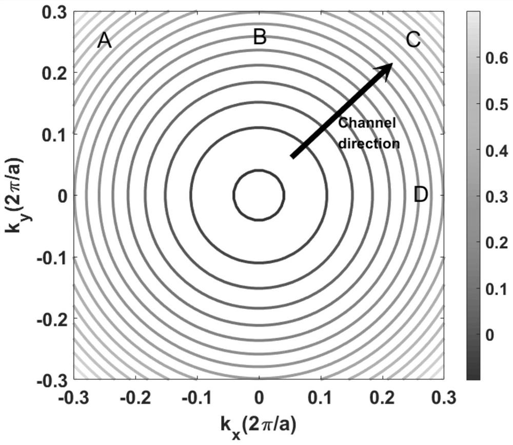
[0059] according to figure 1 As shown, through the EDA algorithm of the present invention, the two-dimensional iso-energy surface diagram of the valence band of the GaN / AlN quantum well grown along the (0001) crystal plane is calculated. The isotropic nature restricts the choice of the best stress type. Therefore, simulations are performed by utilizing uniaxial stresses that can lead to band anisotropy.

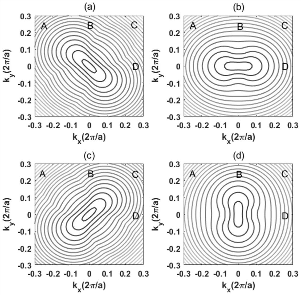
[0060] according to figure 2 As shown, the uniaxial compressive stress shear component directions of 0°, 45°, 90° and 135° are applied to the GaN / AlN heterojunction and the channel direction, respectively. After applying uniaxial compressive stress, the quantum well subband shape changes such as image 3 shown. Under stress, the energy rises or falls, with the lowest energy positions having the highest hole density of states and leading the modulation of hole mobility. Therefore, the change of energy at different positions can be observed from the change of the shape of...


PUM


Abstract

The invention provides a P-type GaN quantum well device transport characteristic EDA algorithm, an application and a simulation method, the EDA algorithm is established based on a k * p perturbation algorithm, simulates a valence band sub-band structure of a GaN / AlN heterojunction quantum well, can be effectively used for simulating the two-dimensional hole gas transport characteristic of the GaN / AlN heterojunction quantum well, can set a plurality of physical effects under the same frame, and can be used for simulating the transport characteristic of the GaN / AlN heterojunction quantum well. Through a quantum mechanics level, a microscopic coupling relationship between parameters such as a plurality of properties and the like and hole mobility is independently analyzed, and an important technical basis is provided for improving transport characteristics of a P-type GaN device.

Description

technical field [0001] The invention relates to the field of GaN materials and devices, in particular to an EDA algorithm, application and simulation method for the transport characteristics of a P-type GaN quantum well device. Background technique [0002] Gallium nitride (GaN) has become a research hotspot due to its wide band gap, high breakdown electric field, high electron mobility, and high electron saturation velocity. And communication systems and other fields have great application prospects. But its low mobility has been. [0003] At present, the research of GaN-based devices mainly focuses on N-type devices. AlGaN / GaN HEMTs can reach 2000 cm without doping. 2 / V s mobility. However, compared with N-type GaN with high transport performance of 2D electron gas, the 2D hole gas mobility of P-type GaN at room temperature has never exceeded 40 cm 2 / V s, this defect has seriously hindered the wide application of GaN in complementary circuits and high-power conversio...

Claims


Application Information

Patent Timeline
Patent Type & Authority Applications(China)
IPC IPC(8): G06F30/23G06N10/20G06F17/18G06F17/16G06F17/11
CPCG06F30/23G06N10/00G06F17/18G06F17/16G06F17/11
Inventor 李希越刘亚群章国豪王峰王靖
Owner SYNERGY INNOVATION INST OF GDUT HEYUAN
Learn More