Semiconductor structure and manufacturing method thereof
A technology of semiconductor and oxide semiconductor, which is applied in semiconductor/solid-state device manufacturing, semiconductor devices, electric solid-state devices, etc. It can solve the problems of reducing high-frequency performance and increasing module size, and achieves the reduction of isolation effect, elimination of parasitic impedance, and compatibility The effect of package design scheme
- Summary
- Abstract
- Description
- Claims
- Application Information
AI Technical Summary
Problems solved by technology
Method used
Image

Examples
Embodiment Construction
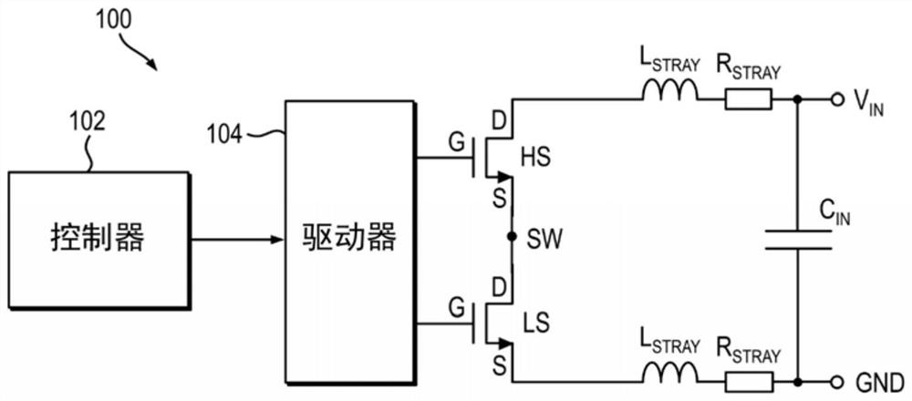
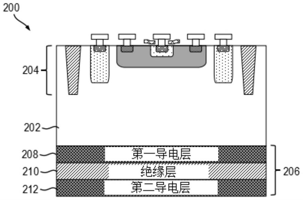
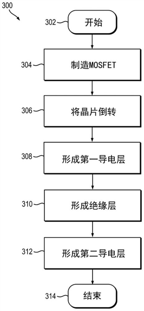
[0038] As shown in one or more embodiments, the principles of the invention will be described herein in the context of various illustrative three-dimensional (3D) structures and methods of fabricating such structures, including low voltage Bipolar devices and CMOS devices and / or circuits, It is provided in a stacked arrangement of high voltage DMOS devices and / or circuits. The 3D structure also includes backside integrated capacitors formed using semiconductor processing steps compatible with CMOS or DMOS processing flows that beneficially eliminate or at least reduce parasitic impedances (particularly inductances) to reduce switching node (SW) noise and voltage peaks, resulting in superior high frequency performance. It should be understood, however, that the present invention is not limited to the particular apparatus and / or methods illustrated and described herein. Rather, various modifications of the embodiments within the scope of the described inventions will appear to ...
PUM
 Abstract
Description
Claims
Application Information
 - R&D Engineer
- R&D Manager
- IP Professional
- Industry Leading Data Capabilities
- Powerful AI technology
- Patent DNA Extraction
Browse by: Latest US Patents, China's latest patents, Technical Efficacy Thesaurus, Application Domain, Technology Topic.
© 2024 PatSnap. All rights reserved.Legal|Privacy policy|Modern Slavery Act Transparency Statement|Sitemap