Medium-free aerial imaging high polymer material and optical lattice device forming process

A polymer material, aerial imaging technology, used in optical components, optics, instruments, etc., can solve the problems of high precision requirements, uneven coating, diffuse reflection of light, etc., to achieve good aging resistance, high light reflection efficiency, The effect of a small thermal expansion coefficient

Pending Publication Date: 2022-08-09
SHENZHEN SAPIENCE TECH CO LTD
View PDF6 Cites 0 Cited by
  • Summary
  • Abstract
  • Description
  • Claims
  • Application Information

AI Technical Summary

Problems solved by technology

[0003] Traditional flat reflectors mostly use glass as the base material. Due to their extremely small size and high requirements for fineness, they have extremely high requirements for structure and optical performance. Therefore, the molding process is complicated, the degree of automation is low, and the cost is high. It is difficult to achieve large-scale
In addition, the glass structure is heavy and fragile, which makes it difficult to store and further restricts its industrialization
In addition to the above two points, this structure needs to be coated with a layer of high reflection film on the surface of the glass. Due to the special surface structure of the glass, the coating is difficult and requires high equipment, which further increases the complexity of the molding process and the cost. high
In addition, there are also some processes that use the integrated molding process to produce an optical projection flat structure, but the coating of the integrally formed structure is difficult, and the inner wall of the structure will cause uneven coating, resulting in diffuse reflection of light, which will greatly increase light loss.

Method used


Image

  • Medium-free aerial imaging high polymer material and optical lattice device forming process
  • Medium-free aerial imaging high polymer material and optical lattice device forming process
  • Medium-free aerial imaging high polymer material and optical lattice device forming process

Examples


Embodiment 1

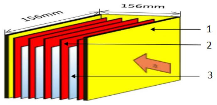
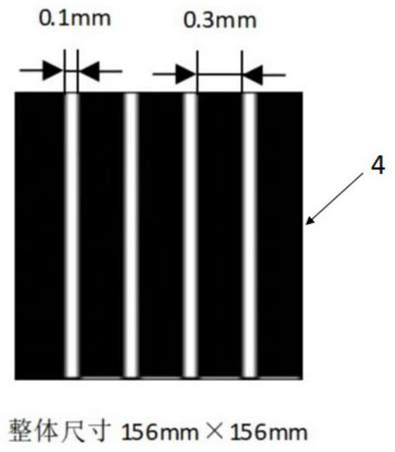
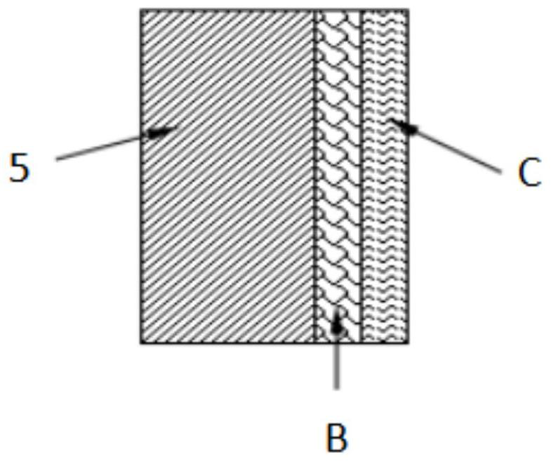
[0063] Embodiment 1 of the present invention provides a medium-free aerial imaging polymer material on the one hand, and the medium-free aerial imaging polymer material includes polymer material A, polymer material B, polymer material C, and polymer material D .

[0064] In parts by weight, the raw materials for preparing the polymer material A include: 40 parts of nano titanium dioxide, 25 parts of dicyclodecane dimethanol acrylate, 15 parts of methyl methacrylate, decaethoxylated bisphenol A dimethacrylate 25 parts of ester, 2 parts of acyl phosphorus photoinitiator, 2 parts of polytetrahydrofuran ether;

[0065] The particle size of the nano titanium dioxide is 30nm;

[0066] The acylphosphorus photoinitiator is 819.

[0067] The preparation process of the polymer material A is as follows: by weight, sequentially adding nano-titanium dioxide, dicyclodecane dimethanol acrylate, methyl methacrylate, decaethoxylated bisphenol A dimethacrylate, and acyl phosphorus The photoi...

Embodiment 2

[0106] Embodiment 2 of the present invention provides a medium-free aerial imaging polymer material on the one hand, and the medium-free aerial imaging polymer material includes polymer material A, polymer material B, polymer material C, and polymer material D .

[0107] In parts by weight, the raw materials for preparing the polymer material A include: 50 parts of nano-titanium dioxide, 30 parts of dicyclodecane dimethanol acrylate, 20 parts of methyl methacrylate, decaethoxylated bisphenol A dimethacrylate 30 parts of ester, 3 parts of acyl phosphorus photoinitiator, 2 parts of polytetrahydrofuran ether;

[0108] The particle size of the nano titanium dioxide is 30nm;

[0109] The acylphosphorus photoinitiator is TPO.

[0110] The preparation process of the polymer material A is as follows: by weight, sequentially adding nano-titanium dioxide, dicyclodecane dimethanol acrylate, methyl methacrylate, decaethoxylated bisphenol A dimethacrylate, and acyl phosphorus The photoi...

Embodiment 3

[0149] Embodiment 3 of the present invention provides a medium-free aerial imaging polymer material on the one hand, and the medium-free aerial imaging polymer material includes polymer material A, polymer material B, polymer material C, and polymer material D .

[0150] In parts by weight, the raw materials for preparing the polymer material A include: 30 parts of nano-titanium dioxide, 20 parts of dicyclodecane dimethanol acrylate, 10 parts of methyl methacrylate, decaethoxylated bisphenol A dimethacrylate 20 parts of ester, 2 parts of acyl phosphorus photoinitiator, 2 parts of polytetrahydrofuran ether;

[0151] The particle size of the nano titanium dioxide is 30nm;

[0152] The acylphosphorus photoinitiator is TPO

[0153] The preparation process of the polymer material A is as follows: by weight, sequentially adding nano-titanium dioxide, dicyclodecane dimethanol acrylate, methyl methacrylate, decaethoxylated bisphenol A dimethacrylate, and acyl phosphorus The photoin...


PUM

PropertyMeasurementUnit
particle diameteraaaaaaaaaa
hardnessaaaaaaaaaa
thicknessaaaaaaaaaa

Abstract

The invention relates to the field of G02B1/04, in particular to a medium-free aerial imaging high polymer material and an optical lattice device forming process, in the application process of a lens material in the field of electronic display, curing forming is fast, safety and environmental protection are achieved, the price is low, and the application range is wide. The high-molecular optical lattice device prepared from the lens material has extremely low thermal expansion coefficient, good weather resistance and aging resistance, and also has high hardness, high toughness and good impact resistance; the device material has a special optical structure, the structure side wall for reflection projection imaging can reach a 12k super mirror surface, the light reflection conduction condition is completely met, a two-dimensional image can be converted into a three-dimensional image, the three-dimensional image is clearly presented in the air, and therefore medium-free aerial imaging is achieved. The method is mainly applied to the electronic display fields of commercial display, vehicle-mounted display, science and technology museums and the like.

Description

technical field [0001] The invention relates to the field of G02B1 / 04, in particular to a medium-free aerial imaging polymer material and a molding process for an optical lattice device. Background technique [0002] Aerial imaging, as a holographic projection technology capable of projecting images into medium-free air, has attracted much attention in recent years. Projecting images into the air through flat plate reflection is one of the means to achieve aerial projection. This technology has the advantages of high image clarity, high color reproduction, and strong stereoscopic effect, and can be widely used in automobiles, TVs, advertising screens, etc. Among them, the projection material is an extremely important part of the reflection projection technology, which directly affects the three-dimensional effect of light and shadow and the performance of image clarity. Therefore, people have been trying their best to seek an imaging material with excellent performance, so...

Claims


Application Information

Patent Timeline
Patent Type & Authority Applications(China)
IPC IPC(8): C08F220/20C08F220/14C08F222/20C08F220/18C08F220/06C08F222/14C09J133/08G02B1/04
CPCC08F220/20C08F222/1025C08F220/1808C08F220/1818C09J133/066G02B1/04C08F220/14C08F220/1811C08F220/06C08F222/102
Inventor 高玉珍叶淑兰王继宝周浩宇
Owner SHENZHEN SAPIENCE TECH CO LTD
Why Eureka
Try Eureka