Flexible solar cell chip and preparation method and application thereof

A flexible solar cell and chip technology, applied in circuits, electrical components, photovoltaic power generation, etc., can solve problems such as easy breakage, battery array failure, and reduced production yield.

Active Publication Date: 2022-08-09
ZHONGSHAN DEHUA CHIP TECH CO LTD
View PDF10 Cites 0 Cited by
  • Summary
  • Abstract
  • Description
  • Claims
  • Application Information

AI Technical Summary

Problems solved by technology

[0003] In the related art, when flexible gallium arsenide solar cells form a solar cell array, in order to avoid the failure of the entire cell array due to problems with a single cell, each cell chip is usually equipped with a bypass diode, and the bypass diode is opposite to the cell chip. Parallel connection. The

Method used


Image

  • Flexible solar cell chip and preparation method and application thereof
  • Flexible solar cell chip and preparation method and application thereof
  • Flexible solar cell chip and preparation method and application thereof

Examples


Example Embodiment

[0167] Example 1

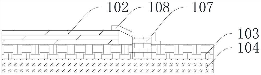
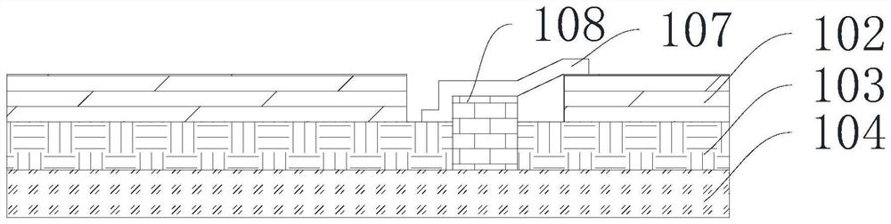
[0168] This embodiment is a flexible solar cell chip and a preparation method thereof.

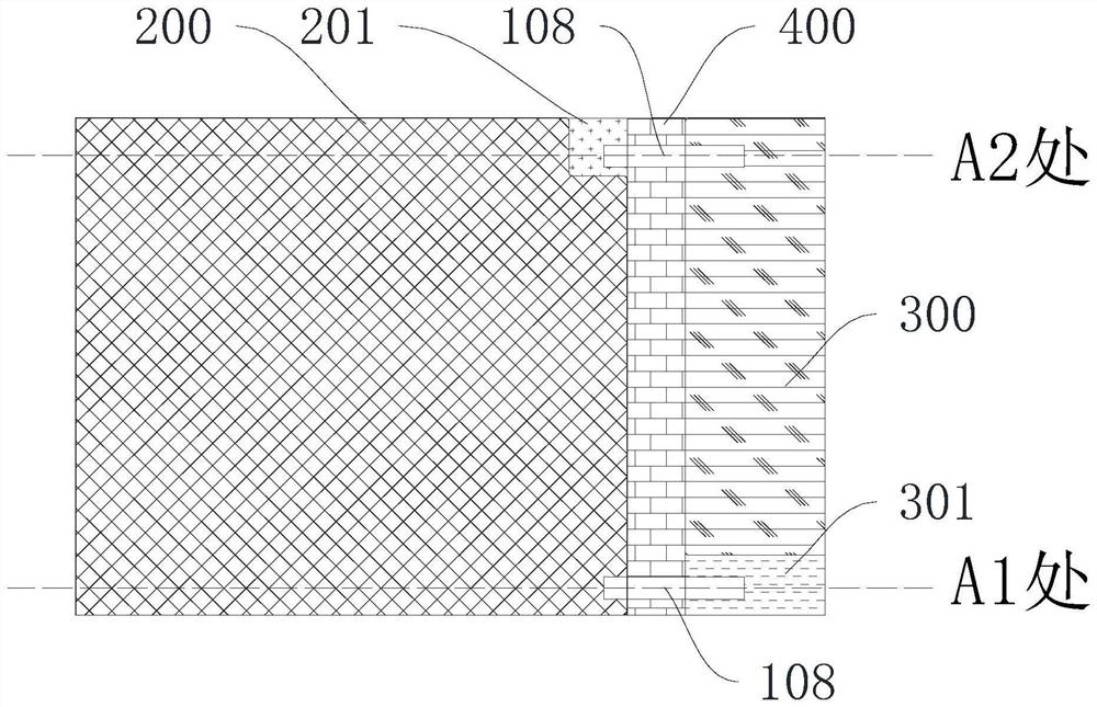
[0169] Top view of the flexible solar cell chip in this embodiment figure 1 , consists of a solar cell epitaxial region 200, a solar cell lower electrode region 201, a diode epitaxial region 300, a diode lower electrode region 301 and an isolation region 400;

[0170] The lower electrode region 201 of the solar cell is electrically connected to the diode epitaxial region 300 through the first interconnecting electrode;

[0171] The solar cell epitaxial region 200 is electrically connected to the diode lower electrode region 301 through the second interconnection electrode;

[0172] The isolation region 400 is used to separate the solar cell epitaxial region 200 and the diode epitaxial region 300 .

[0173] The solar cell epitaxial region 200 is formed by stacking the following film layers in sequence:

[0174] PI layer 104, first metal bonding layer, P-type GaInAs oh...

Example Embodiment

[0229] Example 2

[0230] This embodiment is a flexible solar cell chip and a preparation method thereof.

[0231] The difference between the flexible solar cell chip in this embodiment and Embodiment 1 is:

[0232] The pyrolysis film in Example 1 was replaced with UV glue (NBD-5172K from Nitto).

[0233] The UV glue removal method is as follows: removing the bonding between the organic bonding layer 105 and the PI layer 104 under UV irradiation for 3 minutes.

Example Embodiment

[0234] Example 3

[0235] This embodiment is a flexible solar cell chip and a preparation method thereof.

[0236] The difference between the flexible solar cell chip in this embodiment and Embodiment 1 is:

[0237] The silicon wafer in Example 1 was replaced with a glass wafer.


PUM


Abstract

The invention relates to a flexible solar cell chip and a preparation method and application thereof, and belongs to the technical field of solar cells. The chip comprises a PI layer, a first metal bonding layer and a second metal bonding layer are arranged in partial area of the surface of the PI layer, adhesive layers are arranged in the first metal bonding layer and the second metal bonding layer, the first metal bonding layer and the second metal bonding layer are divided by the adhesive layers, and the adhesive layers are arranged on the PI layer. A first epitaxial layer is arranged in a partial area of the surface of the first metal bonding layer, and a second epitaxial layer is arranged in a partial area of the surface of the second metal bonding layer. According to the flexible solar cell chip, the diode and the solar cell chip are integrally formed; therefore, the treatment process is saved; and the problem of breakage caused in the welding process is avoided, and the production yield is high.

Description

technical field [0001] The invention relates to the technical field of solar cells, in particular to a flexible solar cell chip and a preparation method and application thereof. Background technique [0002] Flexible solar cells have the advantages of adjustable band gap, light weight, high mass specific power, flexibility and bendability, and good surface coverage. [0003] In the related art, when flexible gallium arsenide solar cells form a solar cell array, in order to avoid the failure of the whole cell array due to the failure of a single cell, each cell chip is usually equipped with a bypass diode, and the bypass diode is opposite to the cell chip. In parallel, the bypass diodes used in the related art are generally silicon or gallium arsenide diodes, which need to be welded in parallel with the battery chip. Due to the flexible characteristics of the flexible battery chip, the bypass diode is easily damaged during the welding operation. , reducing the production yie...

Claims


Application Information

Patent Timeline
IPC IPC(8): H01L31/044H01L31/18
CPCH01L31/044H01L31/18Y02P70/50
Inventor 王兵范芳芳王文开张文涛胡丹
Owner ZHONGSHAN DEHUA CHIP TECH CO LTD
Why Eureka
Try Eureka