Storage structure in ferroelectric nonvolatile memory and its read method
A non-volatile memory and ferroelectric technology, applied in static memory, digital memory information, information storage, etc., can solve the problems of shorter information retention time, shorter information retention time, and higher information programming voltage
- Summary
- Abstract
- Description
- Claims
- Application Information
AI Technical Summary
Problems solved by technology
Method used
Image
Examples
no. 1 example
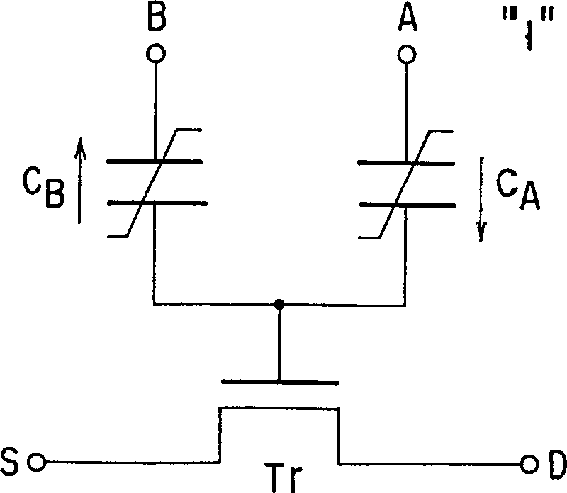
[0050] Figure 2A with 2B It is an equivalent circuit diagram showing the memory cell structure in the ferroelectric nonvolatile memory according to the first embodiment of the present invention.
[0051] Two ferroelectric capacitors C with the same amount of remanent polarization A 、C B One side electrode of the electrode is connected to the gate electrode of the field effect transistor (MOSFET) Tr of MOS structure, and the ferroelectric capacitor C A 、C B The other electrodes are connected to terminals A and B, respectively. Transistor Tr and ferroelectric capacitor C A 、C B form a storage unit. Each ferroelectric capacitor C A 、C B The dielectric film used such as PZT (lead zirconate titanate), and the area and film thickness of the capacitor are set to the same value.
[0052] In this embodiment, the memory cell can be used as an analog memory, but in this example, to simplify its description, an example of its operation is explained where this memory cell is use...
no. 2 example
[0062] Next, a second embodiment of the present invention will be described. This embodiment is similar to the first embodiment in basic construction, but the capacitor C A The film thickness of the ferroelectric film is related to the capacitor C B The film thickness of the ferroelectric film is large enough. For example, if capacitor C B The film thickness of the ferroelectric film is set to about 0.1µm, it is better to set the capacitor C A The film thickness of the ferroelectric film is set to about 0.2-0.3 μm, that is, the capacitor C A The film thickness of the ferroelectric film is the capacitor C B 2 to 3 times the film thickness of the ferroelectric film.
[0063] The programming method of the memory in this embodiment is basically the same as that of the first embodiment, but if the gate capacitance of the MOSFET is large and the influence of the potential on the semiconductor side cannot be ignored, set the potential of the semiconductor to an electrically floa...
no. 3 example
[0072] 4A to 4C are for explaining the configuration of a ferroelectric nonvolatile memory according to a third embodiment of the present invention, wherein a perspective view of a memory cell structure is shown in FIG. 4A, Figure 4B is a graphic plan view showing the overlapped state of the gate electrode and the wiring electrode, and Figure 4C is the equivalent circuit diagram.
[0073] This embodiment is achieved by forming the structure of the first embodiment at a high density using an SOI (silicon on sapphire) substrate.
[0074]On an insulating substrate 31 composed of a silicon substrate and a silicon dioxide film formed thereon, a strip 32 of a single crystal silicon film is formed. A dielectric film 33, such as a silicon dioxide film, is formed on the above structure by deposition. The single crystal silicon thin film strip 32 consists of npn structures divided in the strip direction. In the figure, one unit portion is shown, but actually a plurality of silicon ...
PUM
 Abstract
Description
Claims
Application Information


