Low contact resistance, low light absorption and full angle high reflectance LED electrode
A technology of low contact resistance and light absorption, applied in circuits, electrical components, semiconductor devices, etc., can solve the problems of low contact resistance and low light absorption characteristics of electrodes
- Summary
- Abstract
- Description
- Claims
- Application Information
AI Technical Summary
Problems solved by technology
Method used
Image

Examples
Embodiment approach 1
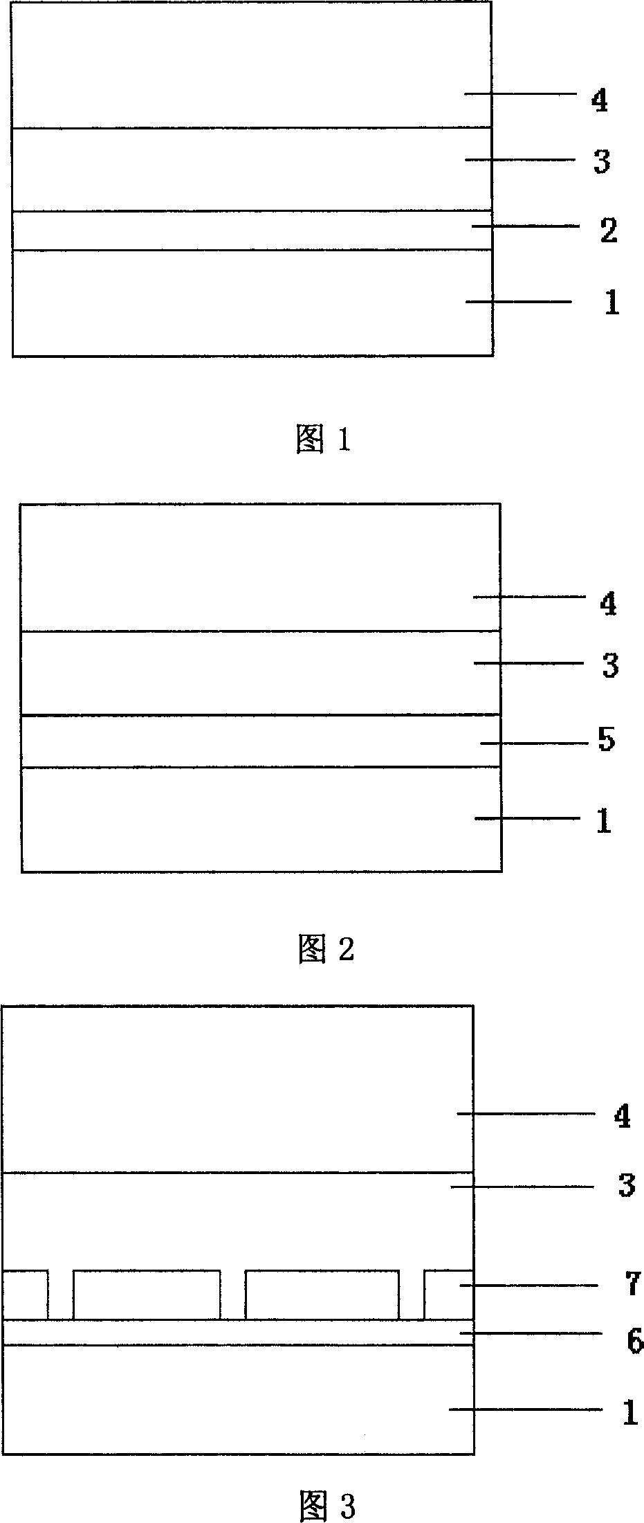
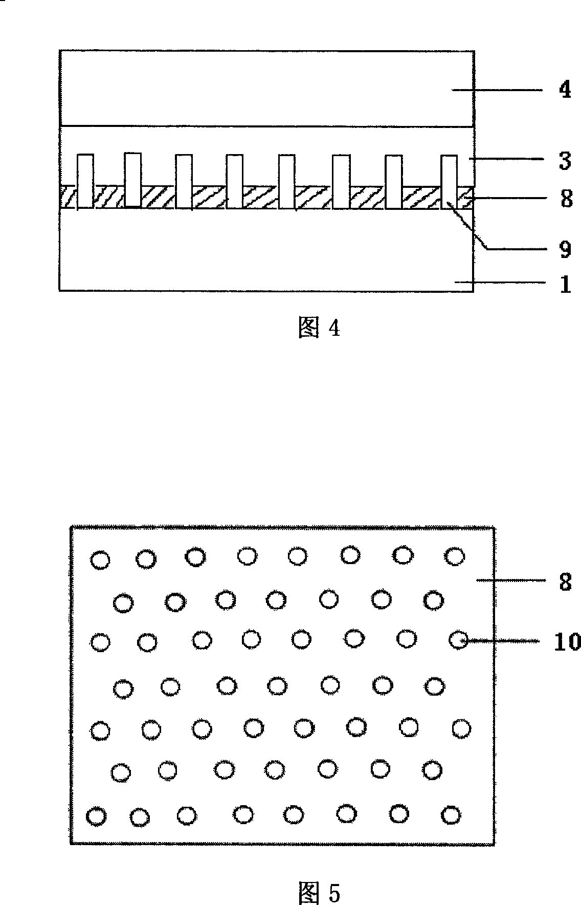
[0021] As shown in Figure 4, the electrode consists of a protective layer Au film 4, an Ag high reflection mirror 3, a porous ohmic contact layer 8, a low refractive index SiO 2 The transparent film 9, the doped semiconductor 1, etc. are composed, and the specific manufacturing steps are as follows:
[0022] 1) A 300 μm × 300 μm LED sample was prepared on a sapphire by a common metal-organic chemical vapor deposition (MOCVD) method. 17 cm -3 .
[0023] 2) The sample is cleaned by common chemical cleaning method: HCl: H 2 The surface of the GaN in the P region was cleaned with a solution of 1:1 O for 5 minutes, and then washed with deionized water for 5 times. After washing with dry N 2 Air dry.
[0024] 3) Put the sample into the reaction chamber of Denton Discovery550 evaporation platform quickly, and pump the reaction chamber to 10 -5 Background vacuum below Pa.
[0025] 4) Plating 2.5nm Ni and 6nm Au at a rate of 2 Ȧ / s at 70°C, using a Karl Suss lithography machine, ...
Embodiment approach 2
[0033] As shown in Figure 4, this electrode is composed of a protective layer Au film 4, an Ag high reflection mirror 3, a porous ohmic contact layer 8, a low refractive index indium tin oxide film 9, and a doped semiconductor 1. The specific manufacturing steps are as follows:
[0034]1) A 300 μm × 300 μm LED sample was prepared on a sapphire by a common metal-organic chemical vapor deposition (MOCVD) method. 17 cm -3 .
[0035] 2) The sample is cleaned by common chemical cleaning method: HCl: H 2 The surface of the GaN in the P region was cleaned with a solution of 1:1 O for 5 minutes, and then washed with deionized water for 5 times. After washing with dry N 2 Air dry.
[0036] 3) Put the sample into the reaction chamber of Denton Discovery550 evaporation platform quickly, and pump the reaction chamber to 10 -5 Vacuum below Pa.
[0037] 4) Plating 4nm Ni at a rate of 3 Ȧ / s at 70°C.
[0038] 5) Using a Karl Suss photolithography machine, a common photolithography proc...
Embodiment approach 3
[0047] 1) A 300 μm × 300 μm LED sample was prepared by the common metal-organic chemical vapor deposition (MOCVD) method, the P-GaN substrate thickness was 1.5 μm, and the Mg doping was 5 × 10 17 cm -3 .
[0048] 2) The sample is cleaned by common chemical cleaning method: HCl: H 2 The surface of the GaN in the P region was cleaned with a solution of 1:1 O for 5 minutes, and then washed with deionized water for 5 times. After washing with dry N 2 Air dry.
[0049] 3) Put the sample into the reaction chamber of Denton Discovery550 evaporation platform quickly, and pump the reaction chamber to 10 -5 Vacuum below Pa.
[0050] 4) Plating 2nm Ni and 2nm Pt at a rate of 3 Ȧ / s at 70°C.
[0051] 5) Using a Karl Suss photolithography machine, a common photolithography process and an etching process are used to make microholes with a radius of 3 μm on the Ni / Pt layer. Microholes communicate with P-GaN. The distance between the centers of adjacent microwells is 22 μm. 20 μm is l...
PUM
 Abstract
Description
Claims
Application Information
PatSnap Eureka turns technology decisions into work you can execute. Powered by our Innovation Knowledge Graph, it runs expert workflows across engineering, life sciences, materials and intellectual property. Get your review-ready output in minutes.


