Etching method for anti-reflecting coating layer on organic substrate

A bottom anti-reflection and coating layer technology, which is applied in the direction of electrical components, semiconductor/solid-state device manufacturing, circuits, etc., can solve the problem that the error of the key dimension of the line width is difficult to grasp, and achieve the effect of improving accuracy

Inactive Publication Date: 2003-08-20
MACRONIX INT CO LTD
View PDF0 Cites 3 Cited by
  • Summary
  • Abstract
  • Description
  • Claims
  • Application Information

AI Technical Summary

Problems solved by technology

However, as long as the organic bottom anti-reflective coating layer is etched by oxygen-containing plasma, even if the lateral etching rate of the photoresist pattern is small, it will maintain a certain rat...

Method used


Image

  • Etching method for anti-reflecting coating layer on organic substrate
  • Etching method for anti-reflecting coating layer on organic substrate
  • Etching method for anti-reflecting coating layer on organic substrate

Examples


Embodiment Construction

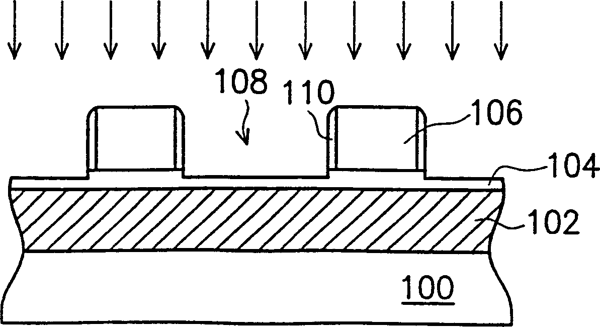
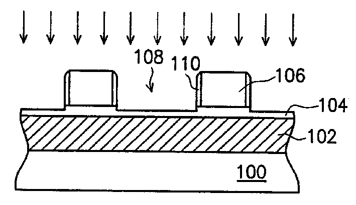
[0018] The invention provides a kind of plasma etching gas for etching the organic bottom anti-reflection coating layer, which is to partially replace the halothane gas (C x h y f z ) as the main etching gas, because part of the replacement of halothane gas can generate halothane polymer on the sidewall of the photoresist pattern to protect the sidewall of the photoresist pattern from lateral etching, so that the gap between the patterns will not become larger and affect the etching critical size. The auxiliary gases used include chlorine, nitrogen, partially substituted halothane gases (for example: methane fluoride (CH 3 F), difluoromethane (CH 2 f 2 ) etc.) or fully substituted fluorine gas (for example: carbon tetrafluoride (CF 4 ), carbon hexafluoride (C 2 f 6 ), three carbon octafluoride (C 3 f 8 ) or tetracarbon octafluoride (C 4 f 8 )Wait).

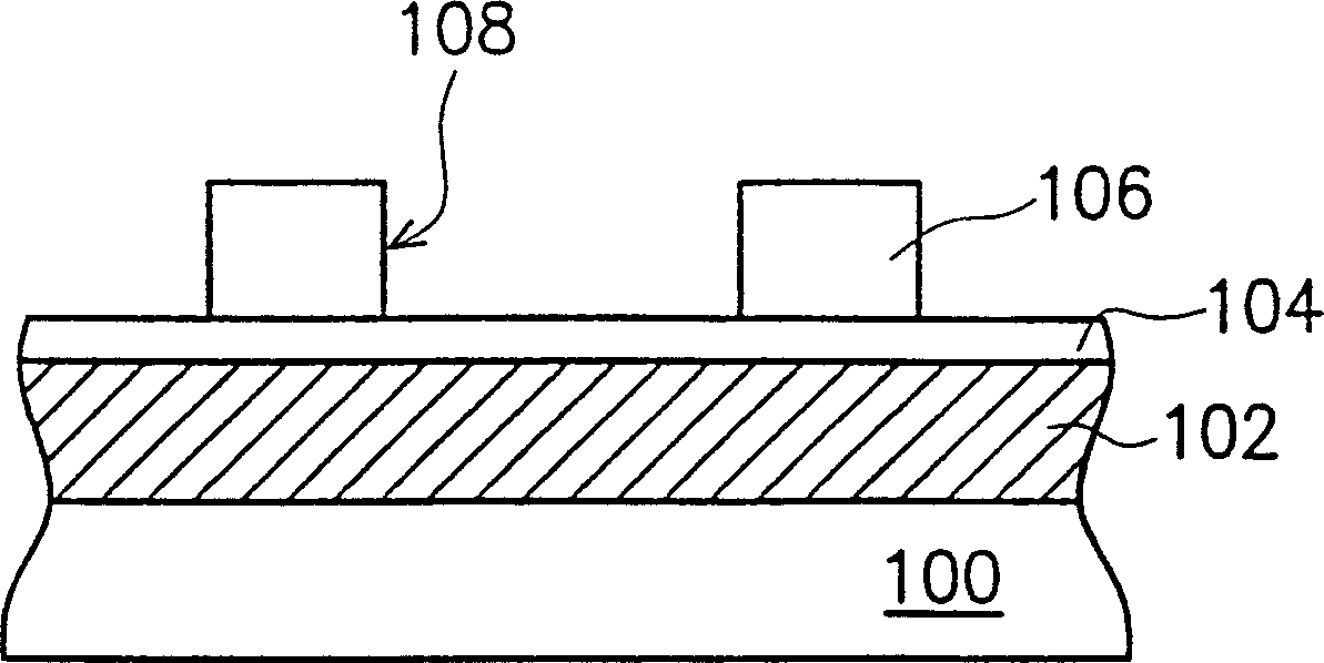
[0019] Figure 1A to Figure 1B It is a cross-sectional view of a process for etching an organic bottom anti-reflecti...


PUM


Abstract

The etching method of the present invention is that after material layer, anti-reflecting base organic coating layer and photoresist pattern are formed successively on the substrate, etching plasma gas including at least partially substituted halothane gas is used to etch the anti-reflecting base organic coating layer. During the etching, halothane polymer is formed on the side wall of the photoresist pattern to prevent the side wall from being etched.

Description

technical field [0001] The present invention relates to a semiconductor manufacturing method, and in particular to an organic bottom anti-reflective coating (Bottom Anti-Reflective Coating, BARC) etching method. Background technique [0002] Photolithography can be said to be one of the most important steps in the entire semiconductor process. Everything related to the metal oxide semiconductor (MOS) device structure, such as the pattern (Pattern) and doped (Dopants) regions of each layer of thin film, is determined by the lithography process. With the increasing integration of integrated circuits, the area of ​​semiconductor elements is gradually reduced, the line width of circuit design is also relatively reduced, and the difficulty of lithography is getting higher and higher. Therefore, before forming the photoresist layer, usually the desired A bottom anti-reflection coating layer (Bottom Anti-Reflection Coating Layer, BARC) is first formed on the etched material layer....

Claims


Application Information

Patent Timeline
IPC IPC(8): G03F7/26G03F7/36
Inventor 梁明中
Owner MACRONIX INT CO LTD
Why Eureka
Try Eureka