

Processing method of nano level saphire substrate and its special polishing liquid
A technology of sapphire substrate and processing method, applied in chemical instruments and methods, other chemical processes, electrical components, etc., can solve the problems of poor surface flatness of sapphire substrate, low diamond tool life, and increased production cost of manufacturers.
- Summary
- Abstract
- Description
- Claims
- Application Information
AI Technical Summary
Problems solved by technology
Method used
Image

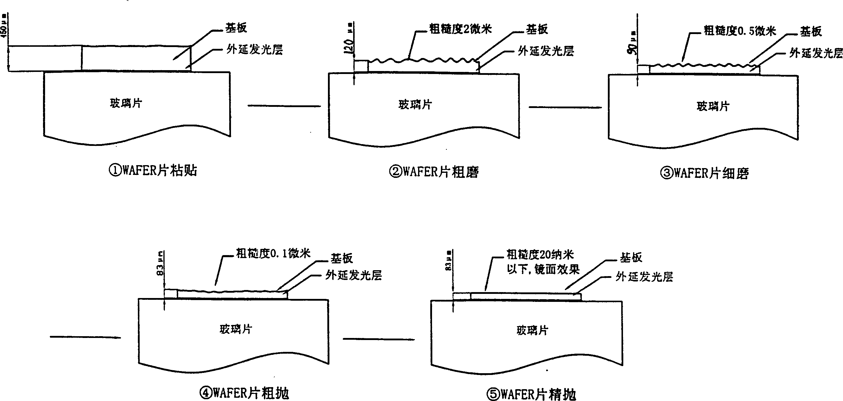
Examples
Embodiment
[0019] Embodiment 1: the content of nano silicon powder is 20%, ethylene glycol is 13%, glycerin is 4%, ethanol ammonia is 0.2%, and deionized water is 62.8%.
[0020] Embodiment 2: the content of nano silicon powder is 23%, ethylene glycol is 10%, glycerin is 3.5%, ethanol ammonia is 0.3%, and deionized water is 63.2%.
[0021] Sample serial number
1
2
3
4
5
routine
63.2
42.2
39.7
45.6
48.8
Recipe 1
15.3
18.1
16.5
18.9
13.2
Recipe 2
16.2
17.3
15.2
17.8
12.8
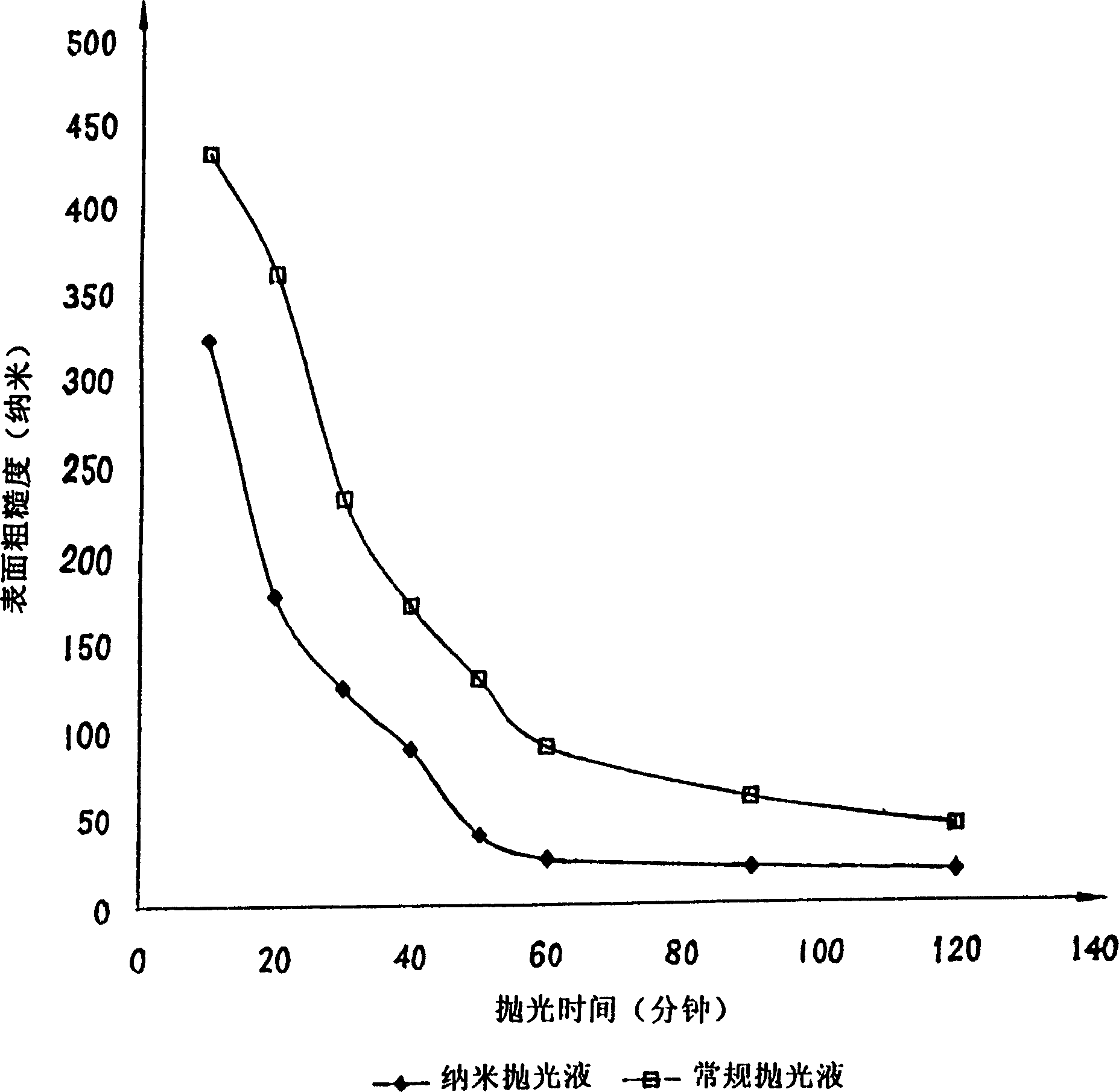
[0022] As can be seen from the above table, when the processing method of the sapphire substrate of the present invention is used in conjunction with the nano-polishing liquid, it is indeed possible to significantly reduce the surface roughness of the sapphire substrate, thereby reaching a high finish (mirror effect) and stress-free (no warpage) , No defor...
PUM
 Abstract
Description
Claims
Application Information