

High dielectric coefficient gate dielectric material hafnium aluminate fil mand preparing method thereof
A technology with high dielectric coefficient and gate dielectric, applied in the field of microelectronic materials, can solve problems such as high grain boundary leakage current, large oxygen diffusivity, and reduce device capacitance, and achieve high thermodynamic stability
- Summary
- Abstract
- Description
- Claims
- Application Information
AI Technical Summary
Problems solved by technology
Method used
Image

Examples
Embodiment 1
[0045] The preparation method of embodiment 1 HAO film, its preparation steps are as follows:
[0046] (1) Preparation of HAO ceramic targets; pure HfO 2 and Al 2 o 3 The powder is mixed according to the molar ratio of 1:1, fully milled by a ball mill for 20 hours, and the mixed powder is cold-pressed into a disc of Φ21mm×4mm under a pressure of 14MPa, and the disc is sintered at 1500°C in a box-type resistance furnace 6 hours to make a dense off-white HAO ceramic target, set aside;
[0047] (2) Selection and treatment of substrate material: use n-type silicon wafer Si(100) with a resistivity of 2Ω.cm. First, put the silicon wafer in acetone and clean it in an ultrasonic machine for 4 minutes. Ultrasonic cleaning with deionized water for 4 minutes, then rinsed with flowing deionized water twice, and finally etched with hydrofluoric acid solution to remove SiO on the surface 2 ,spare;
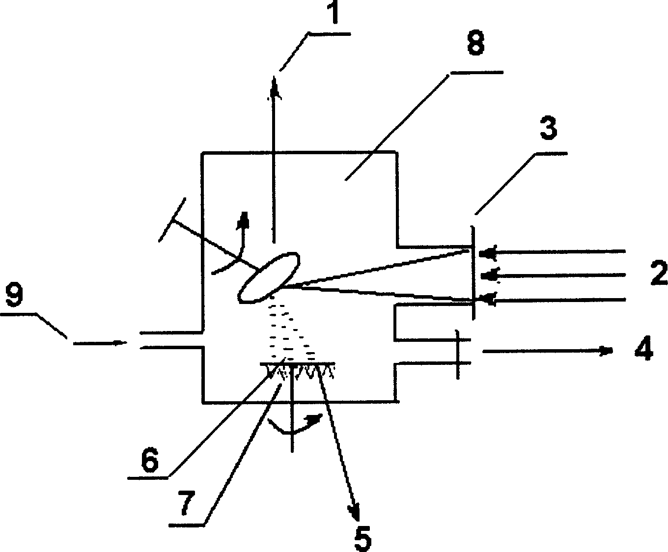
[0048] (3) The HAO ceramic target is placed on the target platform 1, the silicon subst...
PUM
| Property | Measurement | Unit |
|---|---|---|
| electrical resistivity | aaaaa | aaaaa |
| wavelength | aaaaa | aaaaa |
| thickness | aaaaa | aaaaa |
Abstract
Description
Claims
Application Information