Semiconductor device and apparatus for communication system

A communication system and semiconductor technology, applied in semiconductor devices, semiconductor/solid-state device manufacturing, amplifiers with semiconductor devices/discharge tubes, etc., can solve problems such as troublesome repairs, large operating costs, and difficult interface matching.

Inactive Publication Date: 2004-02-18
PANASONIC CORP
View PDF0 Cites 4 Cited by
  • Summary
  • Abstract
  • Description
  • Claims
  • Application Information

AI Technical Summary

Problems solved by technology

[0014] The most important part of the signal amplification components in the above-mentioned previous broadcasting stations, sending and receiving information circuits, etc., are generally formed on GaAs substrates, but because they cannot overcome the compromise of high withstand voltage and low resistance, many components requiring a small power supply are formed. Quantity of components, it is difficult to realize the miniaturization of the device
As a result, in order to maintain the operation of the relay station, a cooling device with a large cooling capacity is required, which requires a large operating cost
In addition, there is a limit to the miniaturization of the circuit when it is applied to a terminal
[0015] In addition, the power amplifier, the most important part of the sending and receiving information circuit, can be equipped with more signal amplification components in the part that needs to implement high-power amplification, but as the frequency of the high-frequency signal increases, it will be repeatedly received from the signal. Interface matching is difficult due to the influence of the reflected wave of the amplifying element
As a result, there will be various problems such as repairing for the purpose of interface adjustment will become very troublesome

Method used


Image

  • Semiconductor device and apparatus for communication system
  • Semiconductor device and apparatus for communication system
  • Semiconductor device and apparatus for communication system

Examples


Embodiment Construction

[0065] best practice

[0066] (Basic configuration of communication system)

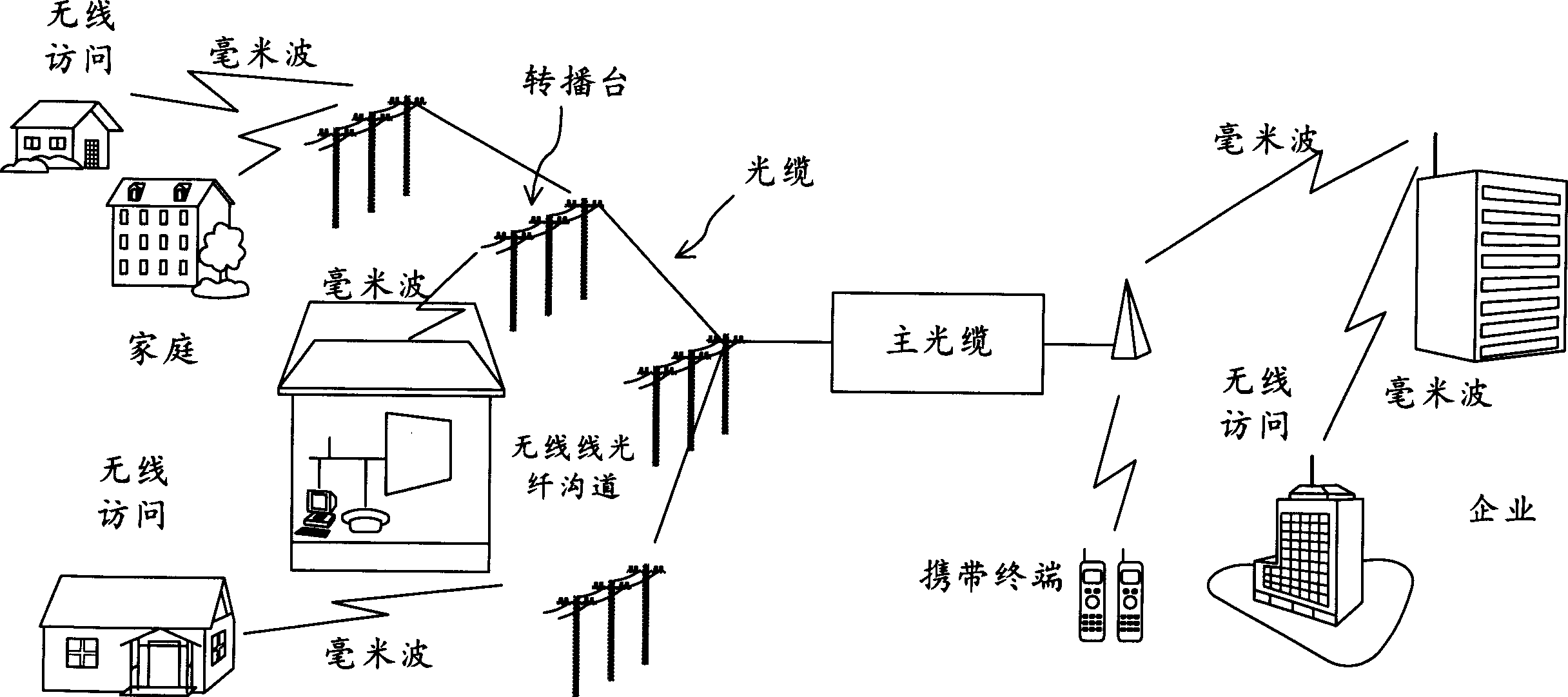
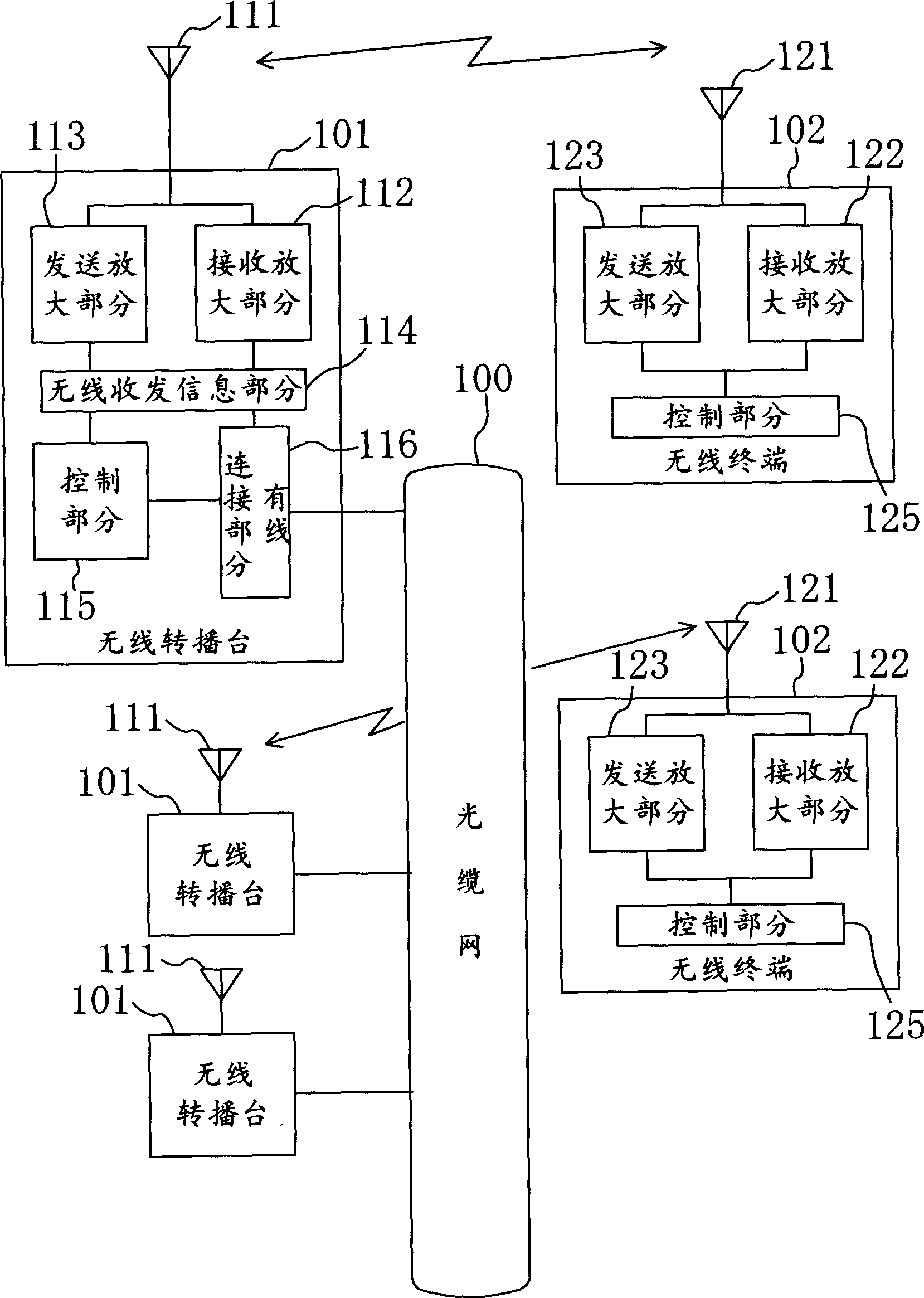
[0067] figure 1It is a perspective view showing an example of the overall concept of a communication system (network system) using millimeter waves according to each embodiment of the present invention. As shown in the figure, relay stations are installed at the ends of the optical fiber lines branched from the trunk line O-fiber. In addition, a wireless communication network has also been established for communicating from each broadcasting station to each home (or office) using millimeter waves. In addition, wireless terminals (mobile stations) in each home or office can use millimeter waves, and it becomes possible to implement various media supply, network communication, and communication between mobile stations from relay stations to devices in each home or office. That is, because the millimeter wave has a wavelength close to light, it is easy to generate an electric wa...


PUM


Abstract

Provided is a semiconductor device of low power consumption and high breakdown voltage and equipment for a communication system using it by mitigating the tradeoff of breakdown voltage increase and resistance reduction. The solution: A HEMT has an InAlAs layer (202), an InGaAs layer (203), a multiple delta-doped InAlAs layer (204) composed of n-type doped layers (204a) and undoped layers (204b) which are alternately stacked, an InP layer (205), a Schottky gate electrode (210), a source electrode (209a), and a drain electrode (209b) on an InP substrate (201). When a current flows in a region (channel region) of the InGaAs layer (203) adjacent the interface between the InGaAs layer (203) and the multiple delta-doped InAlAs layer (204), a breakdown voltage in the OFF state can be increased, while resistance to the movement of carriers passing through the multiple delta-doped InAlAs layer (204) as a carrier supplying layer is reduced.

Description

[0001] technology area [0002] The present invention relates to a semiconductor device having the function of a semiconductor power device used for high voltage and high frequency signals, and an apparatus for a communication system using the semiconductor device. Background technique [0003] In recent years, development of new semiconductor materials (including so-called semi-insulating materials) has been actively carried out for the purpose of realizing semiconductor devices having specific characteristics such as excellent high-frequency characteristics, light emission characteristics, and withstand voltage characteristics. Among semiconductor materials, for example, indium phosphide (InP) is expected to be applied to next-generation high-frequency devices and high-temperature Materials for operating devices, etc. [0004] Generally speaking, the so-called power supply device is a general term for devices that perform larg...

Claims


Application Information

Patent Timeline
Patent Type & Authority Applications(China)
IPC IPC(8): H01L21/8252H01L27/06H01L29/20H01L29/778H03F3/60
CPCH01L21/8252H01L29/7785H01L27/0605H03F3/601H01L29/2003H03F2200/294
Inventor 横川俊哉铃木朝实良出口正洋吉井重雄古屋博之
Owner PANASONIC CORP
Why Eureka
Try Eureka