Al-Ga-In-As multi-quantum sink super radiation luminous diode

A technology of superluminescence and multiple quantum wells, which is applied in the field of aluminum gallium indium arsenic multi-quantum well superluminescent light-emitting diodes, can solve problems such as the unspecified fabrication structure, improve quantum efficiency and high temperature characteristics, and reduce series resistance , Improve the effect of injection efficiency

Inactive Publication Date: 2004-11-24
GUANGXUN SCI & TECH WUHAN
View PDF1 Cites 12 Cited by
  • Summary
  • Abstract
  • Description
  • Claims
  • Application Information

AI Technical Summary

Problems solved by technology

In the 850nm band, US Patent No. 5,521,935 proposes to use AlGaInAs material to make a light-emitting device SLED, but does not give a specific fabrication structure

Method used


Image

  • Al-Ga-In-As multi-quantum sink super radiation luminous diode
  • Al-Ga-In-As multi-quantum sink super radiation luminous diode
  • Al-Ga-In-As multi-quantum sink super radiation luminous diode

Examples


Embodiment Construction

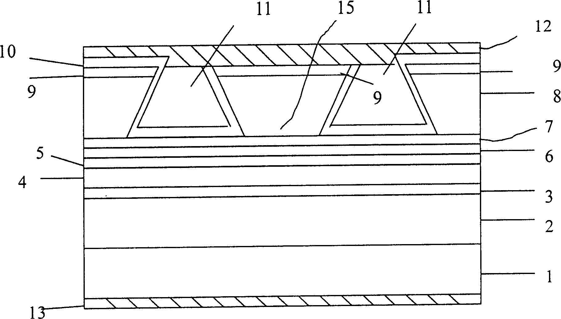
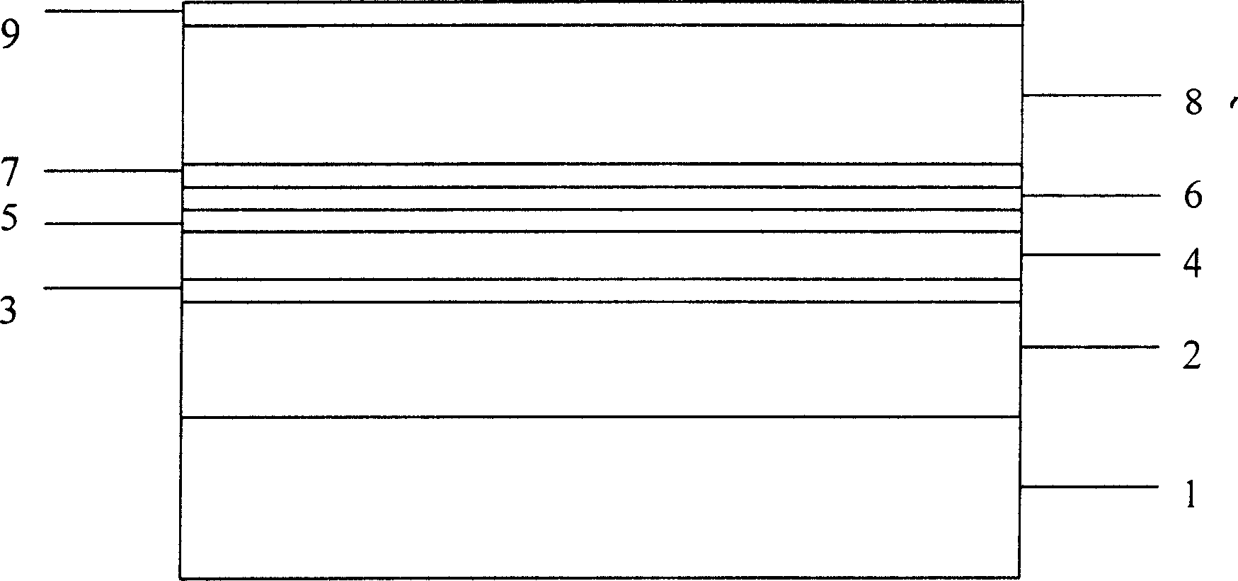
[0018] The AlGaInAs / InP material system is adopted, and the light emitting wavelength range of the active region is 1.25 μm to 1.65 μm. Specifically, it includes the lower cladding layer on the n-type InP substrate, the upper and lower confinement layers (SCH) and the multi-quantum well active region located therein, wherein the thickness of the well is 5-10nm, and the total thickness of the well barrier in the active region Between 10-500nm, the multi-quantum well active region has 4-10 pairs of well barriers.

[0019] Wherein the separate confinement layer is a stepped structure or a slowly changing separate confinement structure (GRIN-SCH), and above the upper confinement layer are an upper cladding layer, an etching cut-off layer, an optical confinement layer and an ohmic contact layer.

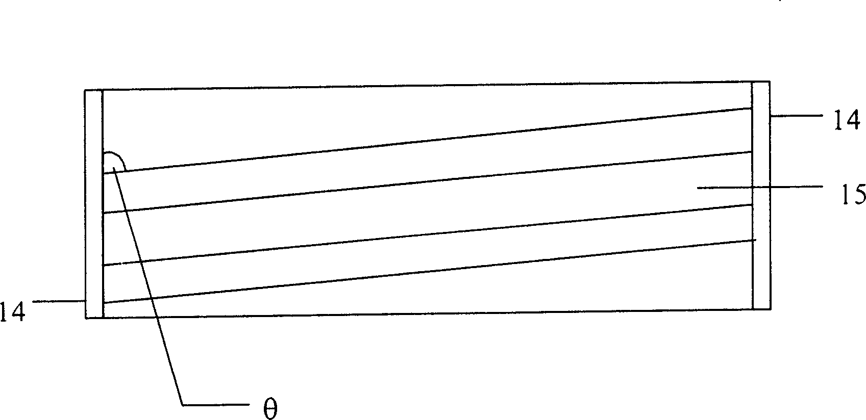
[0020] Usually the RWG structure is a vertical mesa-shaped ridge waveguide, which easily causes the problem of large series resistance of the device. In order to reduce the series resist...


PUM


Abstract

The present invention provides a multi-quantum-well superluminescent diode. It is characterized by that it adopts AlGaInAs/InP materials, the luminescent wavelength range of its active region is 1.25 micrometers to 1.65 micrometers, and on the n-type InP substrate successively are set lower clad, upper and lower respective limiting layers and multi-quantum-well active region positioned in them, in which the thickness of the well is 5-10 nm, and the total thickness of active region well barrier is 10-500 nm. On the upper limiting layer are successively set upper clad, etching cut-off layer, optical limiting layer and ohmic contact layer. It adopts an inverted mesa ridge waveguide structure, its two sides are equipped with polymer plane buried layer respectively, and its upper surface is equipped with plane electrode, in which the included angle theta of waveguide direction and light-outgoing end face of SLED is 75-85 deg.

Description

technical field [0001] The invention relates to an aluminum gallium indium arsenic multi-quantum well superluminescent light-emitting diode. Compared with lasers, the device has a wide spectral range and a large output power compared with light-emitting diodes (LEDs), and the output power etc. The parameters must meet certain requirements and belong to the fields of sensing, optical communication and fiber optic gyro navigation. Background technique [0002] In the fields of communication and sensing, it is necessary to use a wide-spectrum gain device, such as the wide-spectrum light source required in dense wavelength division multiplexing (DWDM) of optical communication systems; in fiber optic gyro navigation based on small incoherence Broad-spectrum light source as required. Generally, lasers (LD) have a small spectral range of a few nanometers (nm). Although LEDs have a wide spectral range, their output power is small, while superluminescent light-emitting diodes have a...

Claims


Application Information

Patent Timeline
Patent Type & Authority Applications(China)
IPC IPC(8): H01L33/00H01S5/343
Inventor 张军常进刘应军甘毅李林松
Owner GUANGXUN SCI & TECH WUHAN
Why Eureka
Try Eureka