Soakage reversibly variable temperature-responsive copolymer film preparation method
A temperature-responsive polymer film technology, applied in the field of temperature-responsive polymer film preparation, can solve the problems of difficult control of molecular structure, inability to achieve reversible control of superhydrophilicity and superhydrophobicity, and achieve excellent wettability The effect of reversible transformation characteristics, simple preparation method and wide applicability
- Summary
- Abstract
- Description
- Claims
- Application Information
AI Technical Summary
Problems solved by technology
Method used
Image
Examples
Embodiment 1
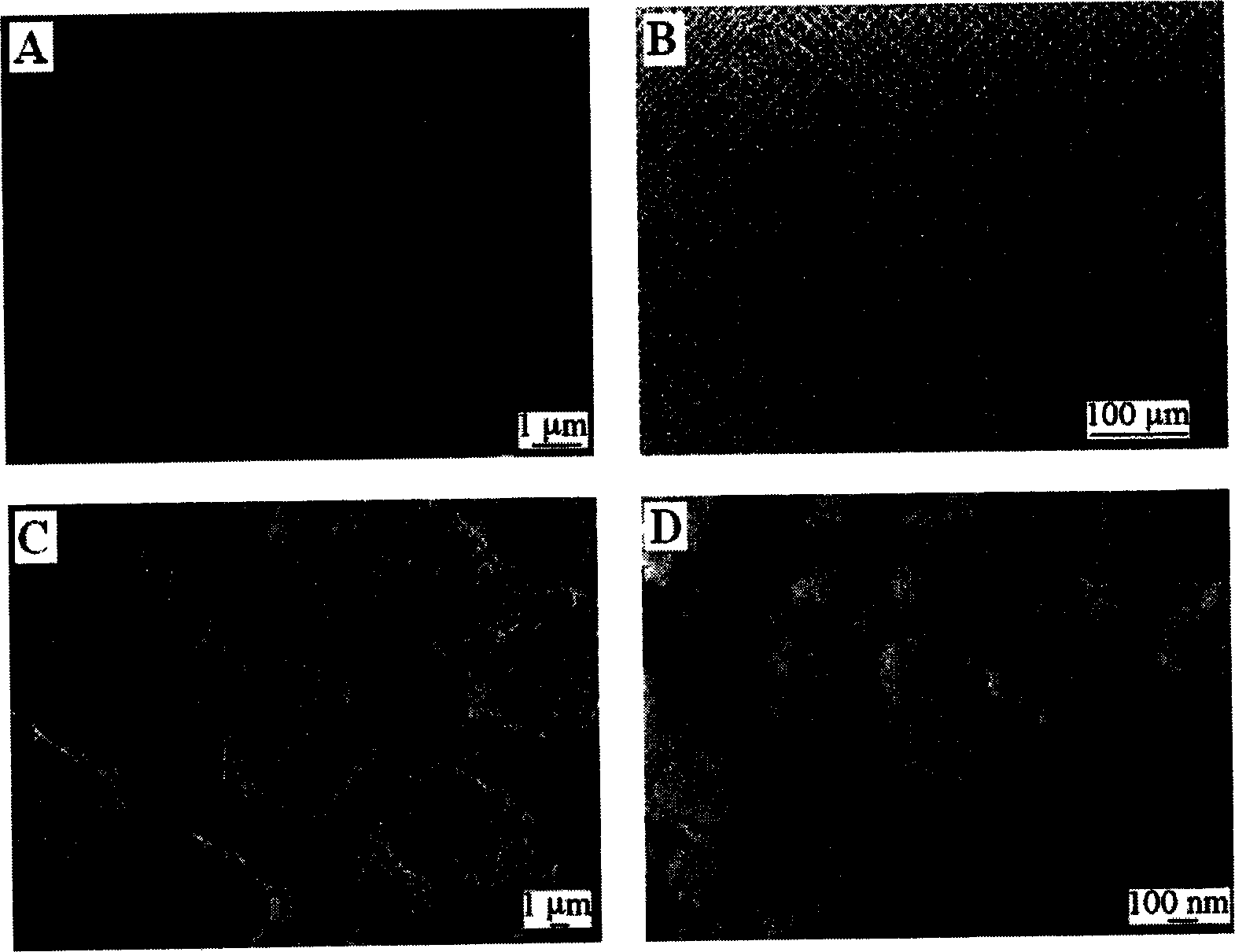
[0048] 1) Soak silicon wafers with chromic acid lotion to remove surface organic impurities; then rinse with deionized water; soak in 0.1N NaOH solution for 2 minutes; 0.1N HNO 3 Soak in solution for 10 minutes.
[0049] 2) The above treated silicon wafer was immersed in 100 mL of toluene solution of 15 wt % trimethoxysilylpropylamine, and heated to reflux for 6 hours. Then rinse with toluene and dichloromethane, and blow dry with nitrogen.
[0050] 3) The above-mentioned treated silicon chip was immersed in 100 mL of chloroform solution of 2 wt % pyridine, 5 mL of 2-bromo-2-methylpropionyl bromide was added, reacted in an ice-water bath for 1 hour, and then continued to react at room temperature for 12 hours. After the reaction, rinse with acetone and dry with nitrogen.
[0051] 4) The above treated silicon wafer was immersed in 200mL of water / methanol (volume ratio 1:5) containing 0.03g CuBr and 0.5mL diethylenetriamine (PMDETA) of 20wt% isopropylacrylamide (NIPAAM). solu...
Embodiment 2
[0054] 1) Soak silicon wafers in chromic acid lotion to remove surface organic impurities; then rinse with deionization; blow dry with nitrogen.
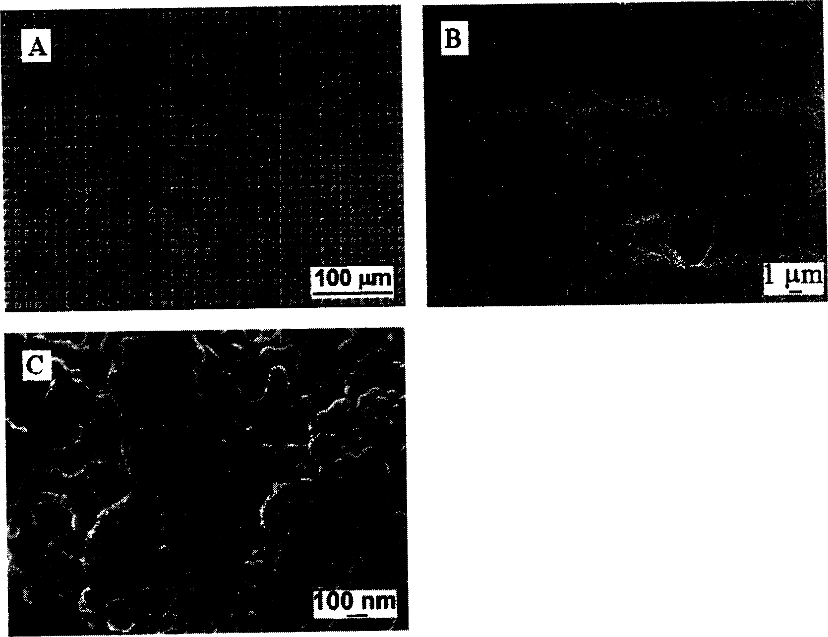
[0055] 2) Horizontally and vertically etch the above-mentioned treated silicon wafer with a laser, the laser etching width is 6 microns, the depth is 5 microns, and the parallel spacing of the laser beams is 8 microns (ie, the etching groove spacing); then use 0.1N NaOH solution Soak for 2 minutes; 0.1N HNO 3 Soak in solution for 10 minutes.
[0056] 3) The above treated silicon wafer was immersed in 100 mL of toluene solution of 15 wt % trimethoxysilylpropylamine, and heated to reflux for 6 hours. Then rinse with toluene and dichloromethane, and blow dry with nitrogen.
[0057] 4) The above-mentioned treated silicon chip was immersed in 100 mL of dichloromethane solution of 2 wt % pyridine, 5 mL of 2-bromo-2-methylpropionyl bromide was added, and reacted in an ice-water bath for 1 hour, then continued to react at room temperature...
Embodiment 3
[0064] 1) Soak silicon wafers in chromic acid lotion to remove surface organic impurities; then rinse with deionization; blow dry with nitrogen.
[0065] 2) Horizontally and vertically etch the above-mentioned silicon wafer with laser, the laser etching width is 6 microns, the depth is 5 microns, and the parallel interval of laser beams is 18 microns (ie, the etching groove spacing); then use 0.1N NaOH solution Soak for 2 minutes; 0.1N HNO 3 Soak in solution for 10 minutes.
[0066] 3) The above-mentioned treated silicon wafer was immersed in 100 mL of toluene solution of 10 wt % trimethoxysilbutylamine, and heated to reflux for 6 hours. Then rinse with toluene and dichloromethane, and blow dry with nitrogen.
[0067] 4) The above-mentioned treated silicon chip was immersed in 100 mL of ethyl acetate solution of 2 wt % pyridine, 5 mL of 2-bromo-2-methylpropionyl chloride was added, reacted in an ice-water bath for 1 hour, and then continued to react at room temperature for 1...
PUM
| Property | Measurement | Unit |
|---|---|---|
| Thickness | aaaaa | aaaaa |
Abstract
Description
Claims
Application Information


