Iron magnetic/anti iron magnet multilayer film pinning system and its preparing method
An anti-ferromagnetic, multi-layer film technology, applied in the direction of magnetic objects, inductors/transformers/magnets, magnetic materials, etc., can solve problems such as easy to be corroded, high coercive force, unsuitable for spin valves and magnetic tunnels , to achieve the effect of good corrosion resistance, ideal resistivity and ideal thermal stability
- Summary
- Abstract
- Description
- Claims
- Application Information
AI Technical Summary
Problems solved by technology
Method used
Image

Examples
Embodiment 1
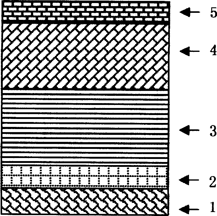
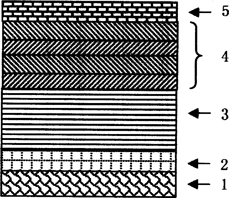
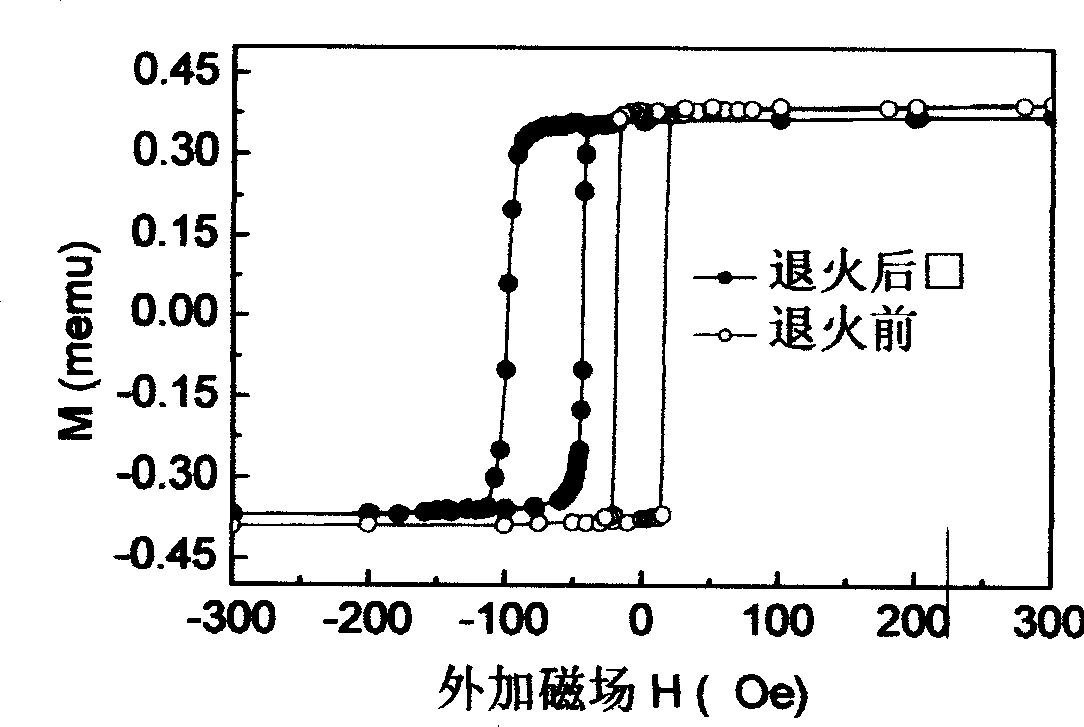
[0030] Such as figure 2 Shown, the structure of ferromagnetic / antiferromagnetic multilayer film pinning material is: glass substrate 1, buffer layer Ta 2, its thickness is 5nm; Ferromagnetic layer Co 0.9 Fe 0.1 3, the thickness of which is 12nm; antiferromagnetic multilayer film [Pt / Cr] 4, wherein the thickness of Pt is 1nm, the thickness of Cr is 0.8nm, the total thickness is about 30nm; and the protective layer Ta 5, the thickness of which is 5nm. The thickness or composition of each layer above is the value when the sample is vacuum deposited or before annealing. image 3 It is the sample preparation state of Example 1 of the present invention and the hysteresis loop measured with a vibrating sample magnetometer after vacuum annealing at 350°C for 5 hours. The coercive force is about 20 Oersted in the preparation state, and there is no nail After annealing, it produces a pinning field of 72 Oersted, and the coercive force only increases slightly, with a value of 28 Oerst...
Embodiment 2
[0032] The structure of the ferromagnetic / antiferromagnetic multilayer pinning system is: substrate Si 1, buffer layer (Ni 0.8 Fe 0.2 ) x Cr 1-x 2, where 0.50.9 Fe 0.1 3. The thickness is 10nm; the antiferromagnetic multilayer film [Pt / Cr] 4, wherein the thickness of Pt is 1nm, the thickness of Cr is 0.8nm, the total thickness is about 30nm; and the protective layer Ta 5, the thickness is 5nm. The thickness or composition of each layer above is the value when the sample is vacuum deposited or before annealing.
Embodiment 3
[0034] The structure of the ferromagnetic / antiferromagnetic multilayer film pinning system is as follows: substrate Si1, buffer layer Ta2, its thickness is 5nm; ferromagnetic layer Co3, its thickness is 10nm; antiferromagnetic layer Cr 0.5 Pt 0.5 4, whose thickness is 20 nm, and the protective layer Ta 5, whose thickness is 5 nm. The thickness or composition of each layer above is the value when the sample is vacuum deposited or before annealing.
[0035] The following takes Example 1 as an example to illustrate the preparation method of the ferromagnetic / CrPt antiferromagnetic multilayer film pinning system of the present invention. The steps of preparing the Co-Fe ferromagnetic / Pt-Cr antiferromagnetic multilayer film pinning system are as follows: firstly, vacuum deposition method is adopted, such as magnetron sputtering method, and the background vacuum degree is better than 10 -5 Pa, and the deposition working pressure under the inert atmosphere is 0.5Pa, the buffer lay...
PUM
| Property | Measurement | Unit |
|---|---|---|
| Thickness | aaaaa | aaaaa |
| Thickness | aaaaa | aaaaa |
| Thickness | aaaaa | aaaaa |
Abstract
Description
Claims
Application Information
 - Generate Ideas
- Intellectual Property
- Life Sciences
- Materials
- Tech Scout
- Unparalleled Data Quality
- Higher Quality Content
- 60% Fewer Hallucinations
Browse by: Latest US Patents, China's latest patents, Technical Efficacy Thesaurus, Application Domain, Technology Topic, Popular Technical Reports.
© 2025 PatSnap. All rights reserved.Legal|Privacy policy|Modern Slavery Act Transparency Statement|Sitemap|About US| Contact US: help@patsnap.com