Method for producing semiconductor device

A manufacturing method and semiconductor technology, applied in the fields of semiconductor/solid-state device manufacturing, semiconductor devices, electric solid-state devices, etc., can solve the problems of high temperature, decrease in electrostatic capacitance of capacitive elements, increase in leakage current of capacitive elements, etc., and achieve high electrostatic capacitance. , to achieve the effect of electrostatic capacitance

Inactive Publication Date: 2005-05-18
PANASONIC CORP
View PDF0 Cites 1 Cited by
  • Summary
  • Abstract
  • Description
  • Claims
  • Application Information

AI Technical Summary

Problems solved by technology

This local non-uniformity of film thickness causes increase or decrease of leakage current in capacitive element, shift of electrostatic capacitance and deterioration of reliability
[0018] Second, although the film thickness of the thermal silicon nitride film 108a based on the thermal nitridation of RTN is an important parameter governing the leakage current flowing through the capacitor element and the reliability of the capacitor element, there is a problem that the film thickness can only be formed in the range of 1nm to 1nm. Problems around 1.5nm
[0019] Thirdly, in the process of removing organic carbon after film formation of the capacitive insulating film 109 made of tantalum oxide and supplying oxygen with a near-stoichiometric composition, from the viewpoint of the crystallization of tantalum oxide, it takes about 60 seconds at 725°C. The heat treatment is sufficient, but from the point of view of oxygen supply, higher temperature is required
Accordingly, adding the silicon oxide film 108b having a dielectric constant smaller than tantalum oxide in series on the film thickness of the capacitive insulating film 109 has a problem that the capacitance of the capacitive element is greatly reduced.

Method used


Image

  • Method for producing semiconductor device
  • Method for producing semiconductor device
  • Method for producing semiconductor device

Examples


Embodiment 1

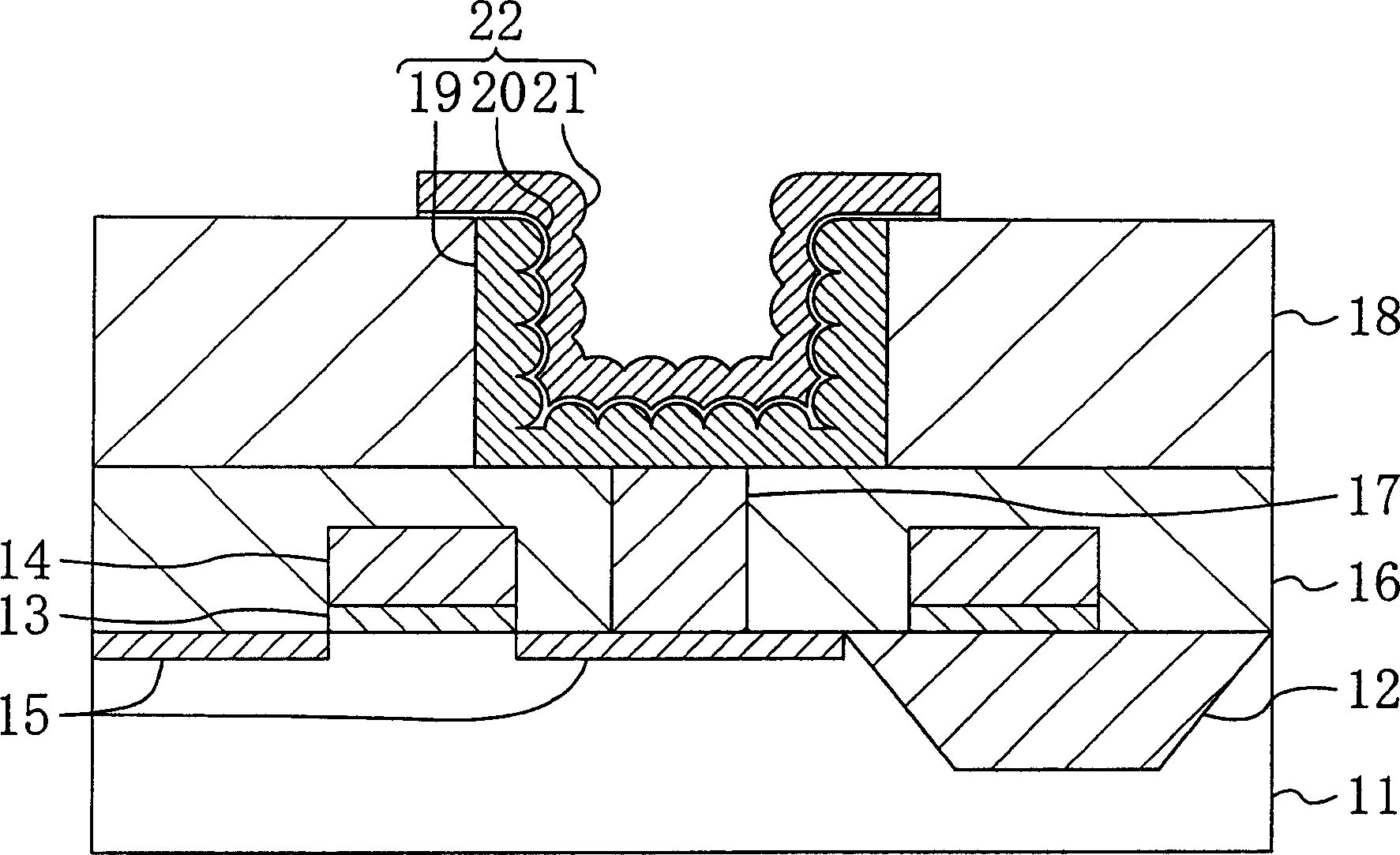
[0080] figure 1 The cross-sectional structure of the main part of the semiconductor device having the capacitor element according to the first embodiment of the present invention is shown. like figure 1 As shown, a semiconductor substrate 11 made of silicon (Si) is divided into element formation regions by an element isolation insulating film 12, and in the divided element formation regions, a gate electrode 14 with a gate insulating film 13 interposed therebetween is formed on the semiconductor substrate. The gate electrodes 14 in the regions on both sides of the gate electrode 14 in 11 constitute an access transistor.

[0081] A first interlayer insulating film 16 is formed on the semiconductor substrate 11 so as to cover the gate electrode 14 and the upper surface is planarized, and a source / drain region 15 of the first interlayer insulating film 16 is formed over one side of the source / drain region 15 and made of conductive polycrystalline silicon. contact plug 17.

...

Embodiment 2

[0111] Next, Embodiment 2 of the present invention will be described with reference to the accompanying drawings.

[0112] Figure 4 A cross-sectional structure of a main part of a semiconductor device having a capacitor element according to Embodiment 2 of the present invention is shown. exist Figure 4 , by for and figure 1 The same constituent members as shown are assigned the same reference numerals, and the description thereof will be omitted.

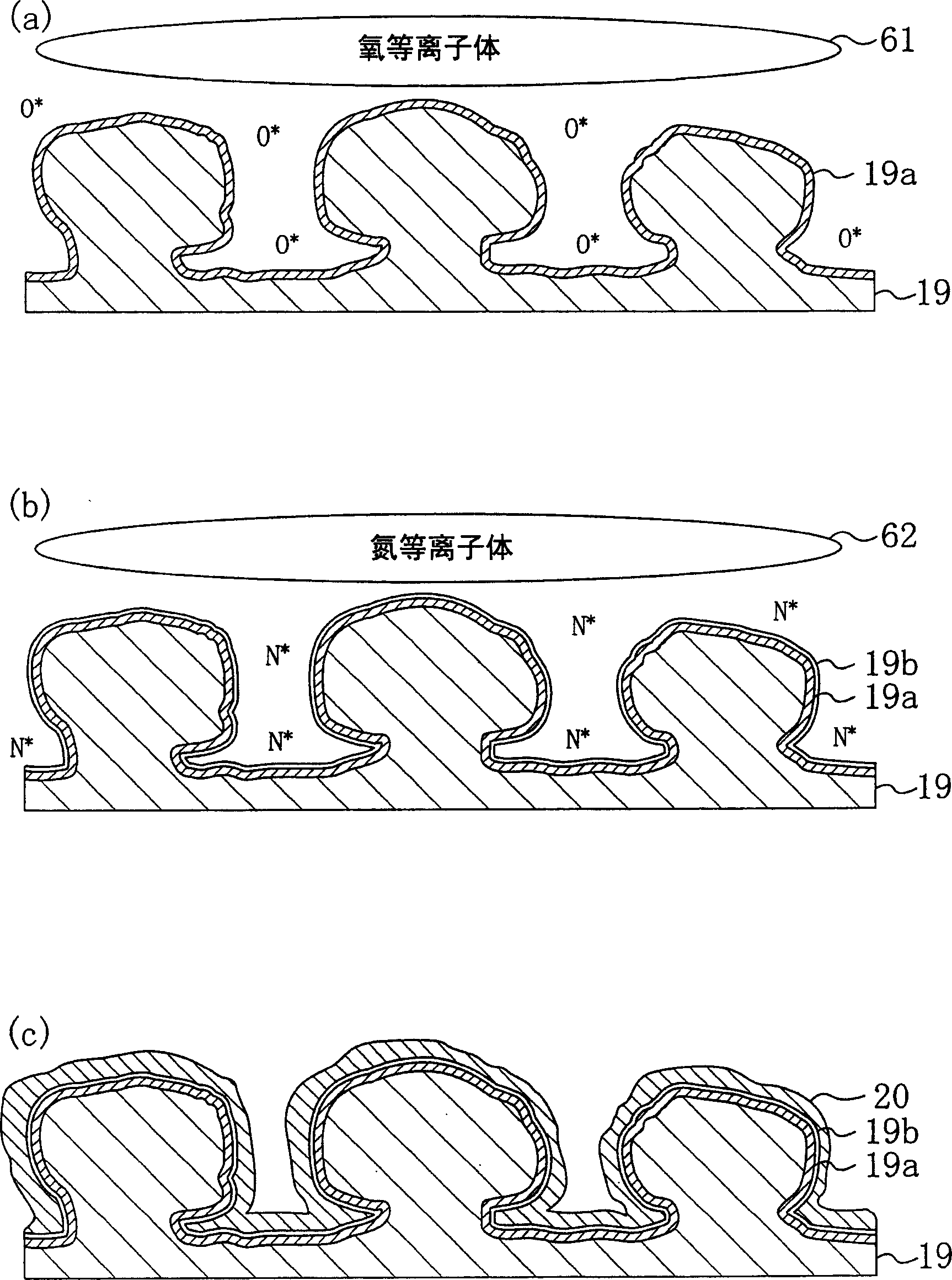
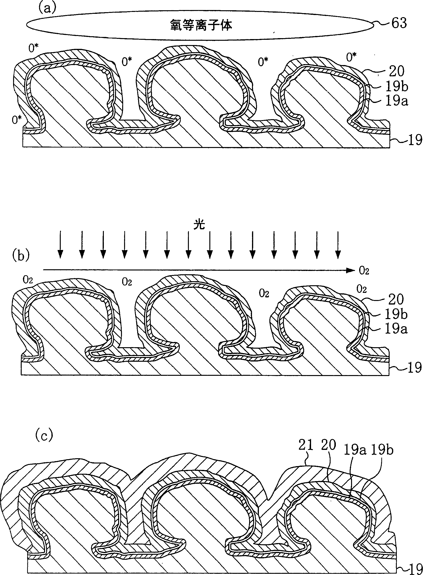
[0113] Example 2 is different from Example 1 in that the structure of the interface layer between the lower electrode 19 and the capacitor insulating film 20 is different, so a method for manufacturing the capacitor element 22 will be described.

[0114] Figure 5 (a) to (c) and Image 6 (a) and (b) are the manufacturing method of the semiconductor device according to the second embodiment of the present invention, that is, part of the amplifying capacitive element, and show the cross-sectional structure of the sequence of s...

Embodiment 3

[0137] Next, Embodiment 3 of the present invention will be described with reference to the accompanying drawings.

[0138] Figure 7 A cross-sectional structure of a main part of a semiconductor device having a capacitor element according to Embodiment 3 of the present invention is shown. exist Figure 7 , for and figure 1 The same constituent members as shown are assigned the same reference numerals, and the description thereof will be omitted.

[0139] Example 3 is different from Example 1 in that the capacitor insulating film 20 has a laminated structure, and therefore, a method for manufacturing the capacitor element 22 will be described.

[0140] Figure 8 (a)~(d), Figure 9 (a) to (c) are cross-sectional structures showing the order of steps of a part of the manufacturing method of the semiconductor device according to Embodiment 3 of the present invention, that is, a part of the amplifying capacitive element.

[0141] First, the lower electrode 19 made of polycry...


PUM

PropertyMeasurementUnit
thicknessaaaaaaaaaa
thicknessaaaaaaaaaa
thicknessaaaaaaaaaa

Abstract

A method of manufacturing a semiconductor device, comprising exposing a lower electrode (19) made of polycrystalline silicon and having a roughened surface to oxygen plasma (61), forming a silicon oxide film (19a) on the surface of the lower electrode (19), By exposing the lower electrode (19) on which the silicon oxide film (19a) is formed to nitrogen plasma (62), the surface of the silicon oxide film (19a) and its vicinity are modified into a silicon nitride film (19b). Next, a capacitive insulating film (20) made of tantalum oxide is formed on the lower electrode (19) on which the silicon nitride film (19b) is formed, and then the capacitive insulating film (20) is exposed to oxygen plasma (63) , oxygen is supplied to the capacitive insulating film (20). Next, the capacitive insulating film (20) is heat-treated in an oxidative atmosphere to crystallize it, and then an upper electrode (21) is formed on the crystallized capacitive insulating film (20).

Description

technical field [0001] The present invention relates to a metal-insulator-semiconductor (MIS) structure in which a metal is used for the upper electrode and a semiconductor for the lower electrode, or a metal-insulator-metal (MIM) structure in which metal is used for both the upper electrode and the lower electrode. A method of manufacturing a semiconductor device that constitutes a capacitor element, particularly a capacitor element of a memory cell, such as a DRAM (Dynamic Random Access Memory) device. Background technique [0002] In a DRAM device, along with an increase in memory capacity, miniaturization of memory cells and peripheral circuits is required. Therefore, the dedicated area of ​​the capacitive elements constituting the memory cells is reduced, and as a result, how to secure the electrostatic capacitance for storing charges in each capacitive element becomes a problem. [0003] Therefore, in order to increase the surface area of ​​the electrode constituting ...

Claims


Application Information

Patent Timeline
Patent Type & Authority Applications(China)
IPC IPC(8): H01L27/04H01L21/02H01L21/314H01L21/316H01L21/321H01L21/44H01L21/82H01L21/822H01L21/8242H01L27/108
CPCH01L21/32105H01L28/84H01L28/60H10B12/03H01L21/022H01L21/3144
Inventor 米田健司
Owner PANASONIC CORP
Why Eureka
Try Eureka