Doped group III-V nitride materials, and microelectronic devices and device precursor structures comprising same

A technology of microelectronic device and device structure, applied in the field of doped III-V group nitride materials, can solve problems such as no satisfactory solution

Inactive Publication Date: 2005-07-20
CREELED INC
View PDF1 Cites 25 Cited by
  • Summary
  • Abstract
  • Description
  • Claims
  • Application Information

AI Technical Summary

Problems solved by technology

[0006] The prior art does not satisfactorily address these problems, which will be addressed in the present invention

Method used


Image

  • Doped group III-V nitride materials, and microelectronic devices and device precursor structures comprising same
  • Doped group III-V nitride materials, and microelectronic devices and device precursor structures comprising same
  • Doped group III-V nitride materials, and microelectronic devices and device precursor structures comprising same

Examples


example 1

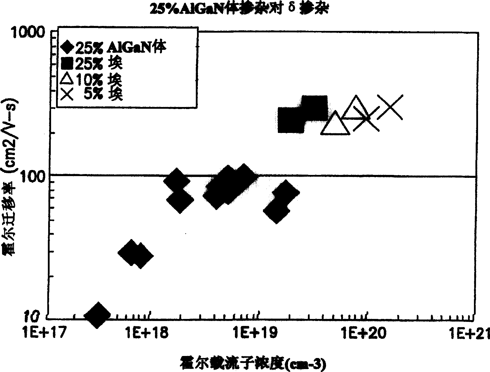
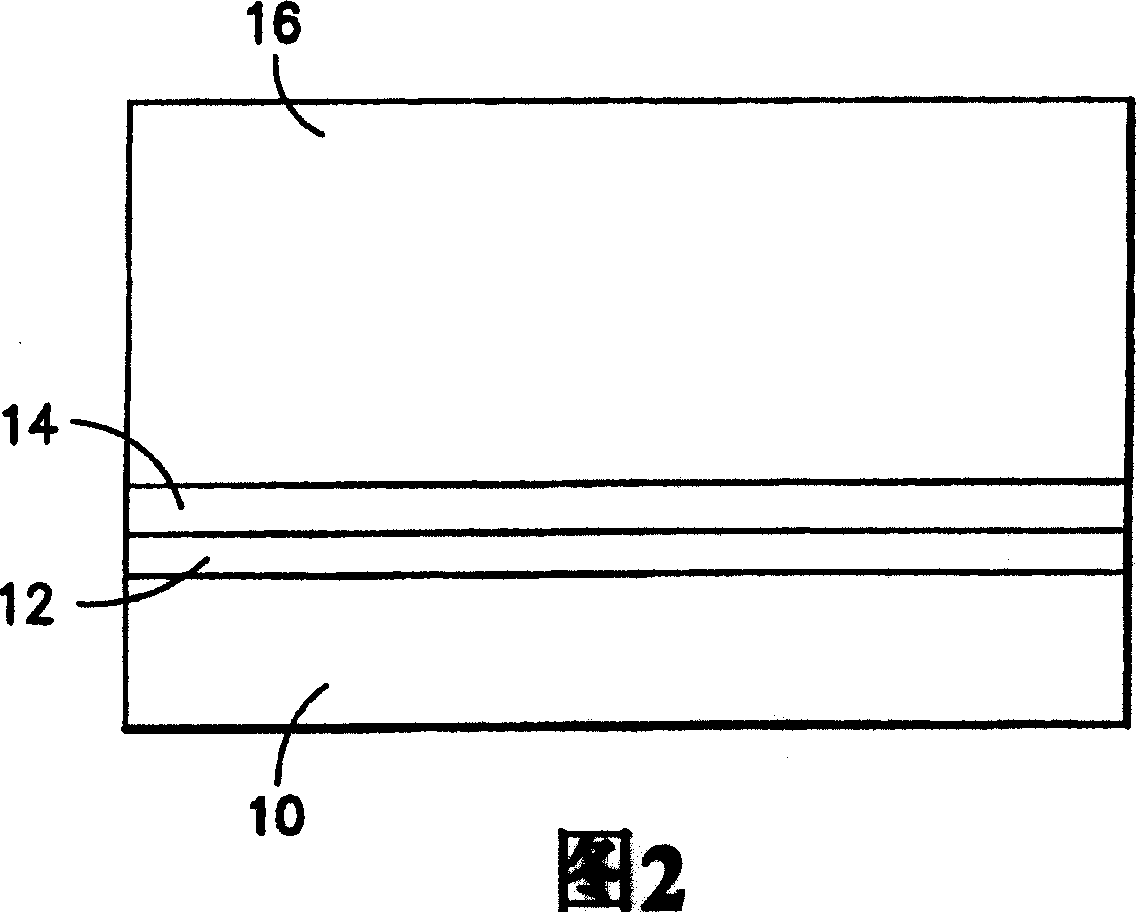
[0129] δ-doped HEMT device structure

[0130] In hydrogen (H 2 ) under a pressure of 100 mbar in an environment, heating the sapphire substrate to 1170° C. for ten minutes. Keeping the pressure constant for the remainder of the delta-doped structure growth, the reactor was cooled to 500°C, and then a low-temperature aluminum nitride (AlN) nucleation buffer layer was deposited in a conventional manner. After the buffer layer is deposited on the sapphire substrate, in 2.5slm ammonia (NH 3 ) and 20slm hydrogen (H 2 ) to a susceptor temperature of 1220° C. and hold this temperature for 2 minutes.

[0131] Trimethylgallium (TMG) was introduced into the reactor at a flow rate sufficient to provide a growth rate of approximately 2.0 μm / hr for 90 minutes, thereby depositing a 3 μm thick gallium nitride (GaN) layer. Trimethylaluminum (TMA) was introduced for 5.5 seconds to grow aluminum gallium nitride (Al 0.25 Ga 0.75 N) Separate layer.

[0132] In the next step, the pre-susp...

example 2

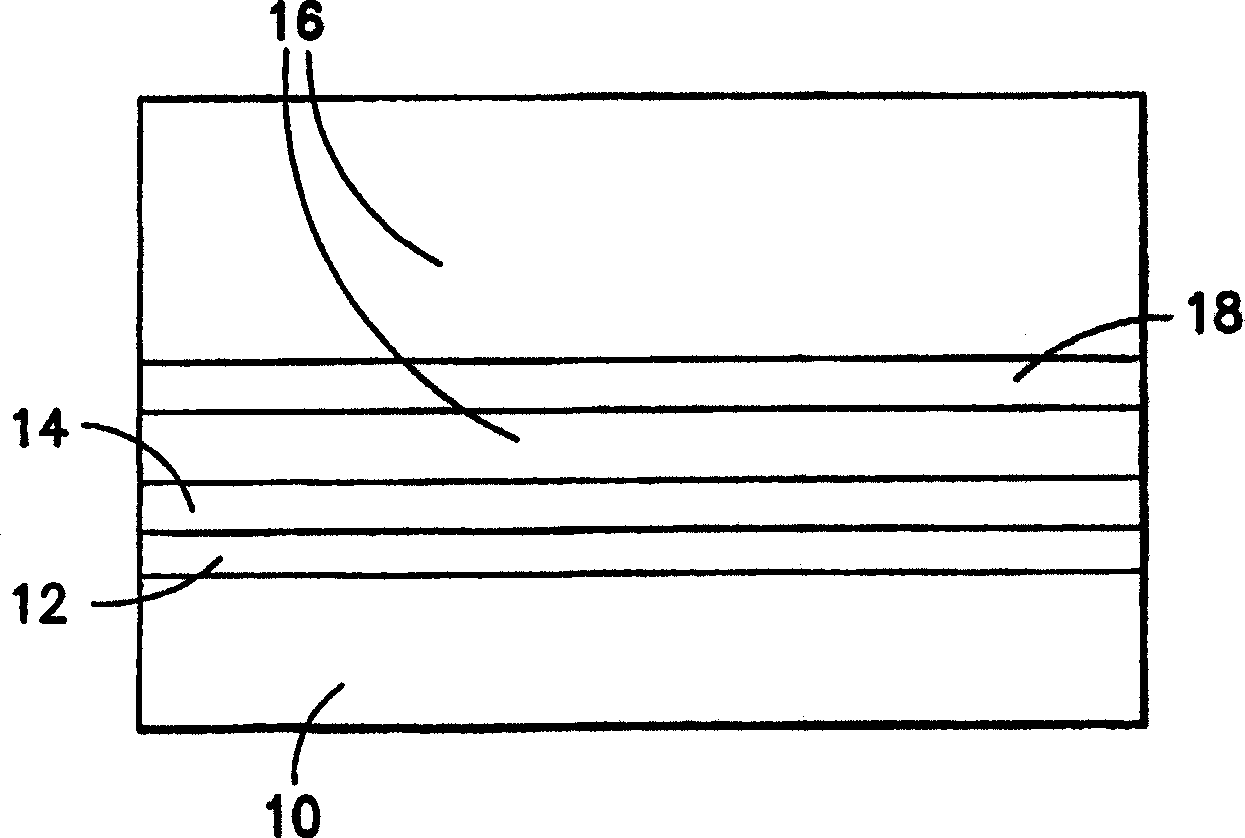
[0135] δ-doped superlattice structure

[0136] In hydrogen (H 2 ) under a pressure of 100 mbar in an environment, heating the sapphire substrate to 1170° C. for ten minutes. Keeping the pressure constant for the remainder of the delta-doped structure growth, the reactor was cooled to 500°C, and then a low-temperature aluminum nitride (AlN) nucleation buffer layer was deposited in a conventional manner. After the buffer layer is deposited on the sapphire substrate, in 2.5slm ammonia (NH 3 ) and 20slm hydrogen (H 2 ) to a susceptor temperature of 1220° C. and hold this temperature for 2 minutes.

[0137] Trimethylgallium (TMG) was introduced into the reactor at a suitable flow rate to provide a growth rate of approximately 2.0 μm / hr for 90 minutes, thereby depositing a 3 μm thick gallium nitride (GaN) layer. Trimethylaluminum (TMA) was introduced at an appropriate flow rate to grow AlGaN (Al 0.2 Ga 0.8 N) layer.

[0138] In the next step, the pre-suspension step was ini...

example 3

[0142] Photocathode structure

[0143] In hydrogen (H 2 ) environment and under a pressure of 100 mbar, the sapphire substrate was heated to 1170° C. for ten minutes. Keeping the pressure constant for the remainder of the delta-doped structure growth, the reactor was cooled to 500°C, and then a low-temperature aluminum nitride (AlN) nucleation buffer layer was deposited in a conventional manner. After the AlN buffer layer was deposited on the sapphire substrate, ammonia (NH 3 ) and hydrogen at a flow rate of 20slm (H 2 ) to a susceptor temperature of 1220° C. and hold this temperature for 2 minutes. Trimethylgallium (TMG) and trimethylaluminum (TMA) were introduced into the reactor to grow AlGaN (Al 0.3 Ga 0.7 N) layer. In the next step, the pre-suspension step was initiated by turning off TMG and TMA entering the reactor, placing the interface at a susceptor temperature of 1220 °C under ammonia gas (NH 3 ) and hydrogen (H 2 )Environment. Steps last 10 seconds befor...


PUM

PropertyMeasurementUnit
thicknessaaaaaaaaaa
thicknessaaaaaaaaaa

Abstract

A Group III-V nitride microelectronic device structure including a delta doped layer and / or a doped superlattice. A delta doping method is described, including the steps of: depositing semiconductor material on a substrate by a first epitaxial film growth process; terminating the deposition of semiconductor material on the substrate to present an epitaxial film surface; delta doping the semiconductor material at the epitaxial film surface, to form a delta doping layer thereon; terminating the delta doping; resuming deposition of semiconductor material to deposit semiconductor material on the delta doping layer, in a second epitaxial film growth process; and continuing the semiconductor material second epitaxial film growth process to a predetermined extent, to form a doped microelectronic device structure, wherein the delta doping layer is internalized in semiconductor material deposited in the first and second epitaxial film growth processes.

Description

technical field [0001] The present invention relates to doped III-V group nitride materials, such as aluminum gallium nitride (AlGaN), gallium nitride (GaN), indium gallium nitride (InGaN) and other materials, and to the preparation methods of these materials, and by These materials constitute microelectronic devices and device precursor structures. Background technique [0002] III-V nitride semiconductors have great potential as useful materials in high-temperature, high-frequency and high-power microelectronics and ultraviolet / blue / green optoelectronics because of their wide bandgap, high thermal conductivity rate and a large electrical breakdown field. [0003] Microelectronic device applications include AlGaN-GaN multilayer laser diodes, high electron mobility transistors (HEMTs), field effect transistors (FETs), heterojunction bipolar transistors (HBTs), light emitting diodes (LEDs) and ultraviolet photodetectors , and common (Al, In, Ga)N substrate devices, which in...

Claims


Application Information

Patent Timeline
Patent Type & Authority Applications(China)
IPC IPC(8): H01L21/331H01L21/205H01L21/338H01L29/15H01L29/20H01L29/36H01L29/737H01L29/778H01L29/812H01L33/02H01S5/30H01S5/323
CPCH01L33/025H01L29/7784H01S5/305H01L29/2003H01S5/32341H01L29/365H01L29/155
Inventor 杰斯里斯·S·弗林乔治·R·布兰德斯
Owner CREELED INC
Why Eureka
Try Eureka