Epitaxial structure of gallium nitride series compound semiconductor and mfg. method

An epitaxial structure, gallium nitride-based technology, applied in semiconductor/solid-state device manufacturing, semiconductor devices, electrical components, etc., can solve the problem of difficult control of production pass rate, reduction of electronic activity, and difficulty of controlling the uniformity of silicon nitride micromasks and density issues, to achieve the effect of improving efficiency and service life, and low crystal structure

Inactive Publication Date: 2005-10-05
SUPERNOVA OPTOELECTRONICS
View PDF3 Cites 14 Cited by
  • Summary
  • Abstract
  • Description
  • Claims
  • Application Information

AI Technical Summary

Problems solved by technology

[0002] The light-emitting component is composed of various material layers. When making each layer of material by epitaxy, there will inevitably be defects in the crystal structure, which will have the following effects on the light-emitting component: 1. Reduce the luminous efficiency
2. Reduce electronic activity
4. V-shaped grooves will appear in the quantum wells of the active layer, and these V-shaped grooves are the origin of dislocations
According to the technology disclosed in this patent, it controls the reaction precursor SiH 4 and NH 3 The better crystallinity of subsequent epitaxial film formation can be achieved by using the flow rate and reaction time, but its disadvantage is that it is not easy to control the uniformity and density of the silicon nitride micromask, so it is not easy to control its production pass rate

Method used


Image

  • Epitaxial structure of gallium nitride series compound semiconductor and mfg. method
  • Epitaxial structure of gallium nitride series compound semiconductor and mfg. method
  • Epitaxial structure of gallium nitride series compound semiconductor and mfg. method

Examples


Embodiment Construction

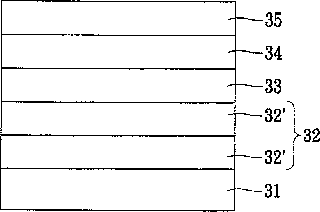
[0027] In view of the shortcomings of common techniques, the present invention proposes an epitaxial structure of GaN-based compound semiconductors. see image 3 , the epitaxial structure 30 of the present invention includes a substrate 31 , a first GaN buffer layer 32 , a second InGaN buffer layer 33 and a GaN epitaxial layer 34 . In the epitaxial structure 30, the substrate 31 is made of one of sapphire, SiC, ZnO and Si, and the first gallium nitride buffer layer 32 further includes a low-temperature gallium nitride buffer layer 32' from bottom to top and a high-temperature GaN buffer layer 32 ″. In addition, the epitaxial structure 30 may further include a GaN-based epitaxial layer 35 on the GaN epitaxial layer 34 .

[0028] see Figure 4 , which illustrates a flow chart of a method of fabricating the epitaxial structure of the present invention. Firstly, a substrate 31 is provided, and the surface of the substrate 31 is thermally cleaned (step 41); then the low-temperat...


PUM

PropertyMeasurementUnit
thicknessaaaaaaaaaa
thicknessaaaaaaaaaa
thicknessaaaaaaaaaa

Abstract

The epitaxial structure comprises following parts: a substrate; a first buffer layer of gallium nitride formed on the substrate; a second buffer layer of gallium indium nitride formed on the first buffer layer; and a epitaxial layer of gallium nitride formed on the second buffer layer. Steps for preparing the structure are as following: forming the first buffer layer of gallium nitride on the substrate at first temperature through epitaxy; forming second buffer layer of gallium indium nitride on the first buffer layer at second temperature; in procedure of raising temperature to third temperature, carrying out surface treatment by maintaining predecessor of trimethyl aluminum and ammonia on second buffer layer; finally, epitaxial layer of gallium nitride is developed at third high temperature. Advantages are: perfective crystal structure and lower density of defects increase efficiency and lifetime of subassembly.

Description

technical field [0001] The invention relates to a semiconductor epitaxial structure and a manufacturing method, in particular to an epitaxial structure of gallium nitride-based compound semiconductors and a method for growing an epitaxial layer of a buffer layer structure. Background technique [0002] Light-emitting components are composed of layers of various materials. During epitaxial fabrication of each layer of material, defects will inevitably occur in the crystal structure, which will have the following effects on the light-emitting component: 1. Reduce luminous efficiency. 2. Reduce electronic activity. 3. Increase the way of dopant ion diffusion. 4. V-shaped grooves appear in the quantum wells of the active layer, and these V-shaped grooves are the origin of dislocations. 5. Increase the initial reverse bias current. In addition, if the crystallization is incomplete and there are cracks or gaps, it is not suitable to grow light-emitting devices above the cracks ...

Claims


Application Information

Patent Timeline
Patent Type & Authority Applications(China)
IPC IPC(8): H01L21/20H01L33/00
Inventor 洪详竣赖穆人
Owner SUPERNOVA OPTOELECTRONICS
Why Eureka
Try Eureka