LED structure

A technology of light-emitting diodes and light-emitting layers, which is applied to electrical components, circuits, semiconductor devices, etc., and can solve problems such as increased stress in multiple quantum well structures

Active Publication Date: 2006-03-15
FORMOSA EPITAXY INCORPORATION +1
View PDF0 Cites 11 Cited by
  • Summary
  • Abstract
  • Description
  • Claims
  • Application Information

AI Technical Summary

Problems solved by technology

What's more, its AlInGaN lattice constant matches the potential well, which can solve the problem

Method used


Image

  • LED structure
  • LED structure
  • LED structure

Examples


no. 1 example

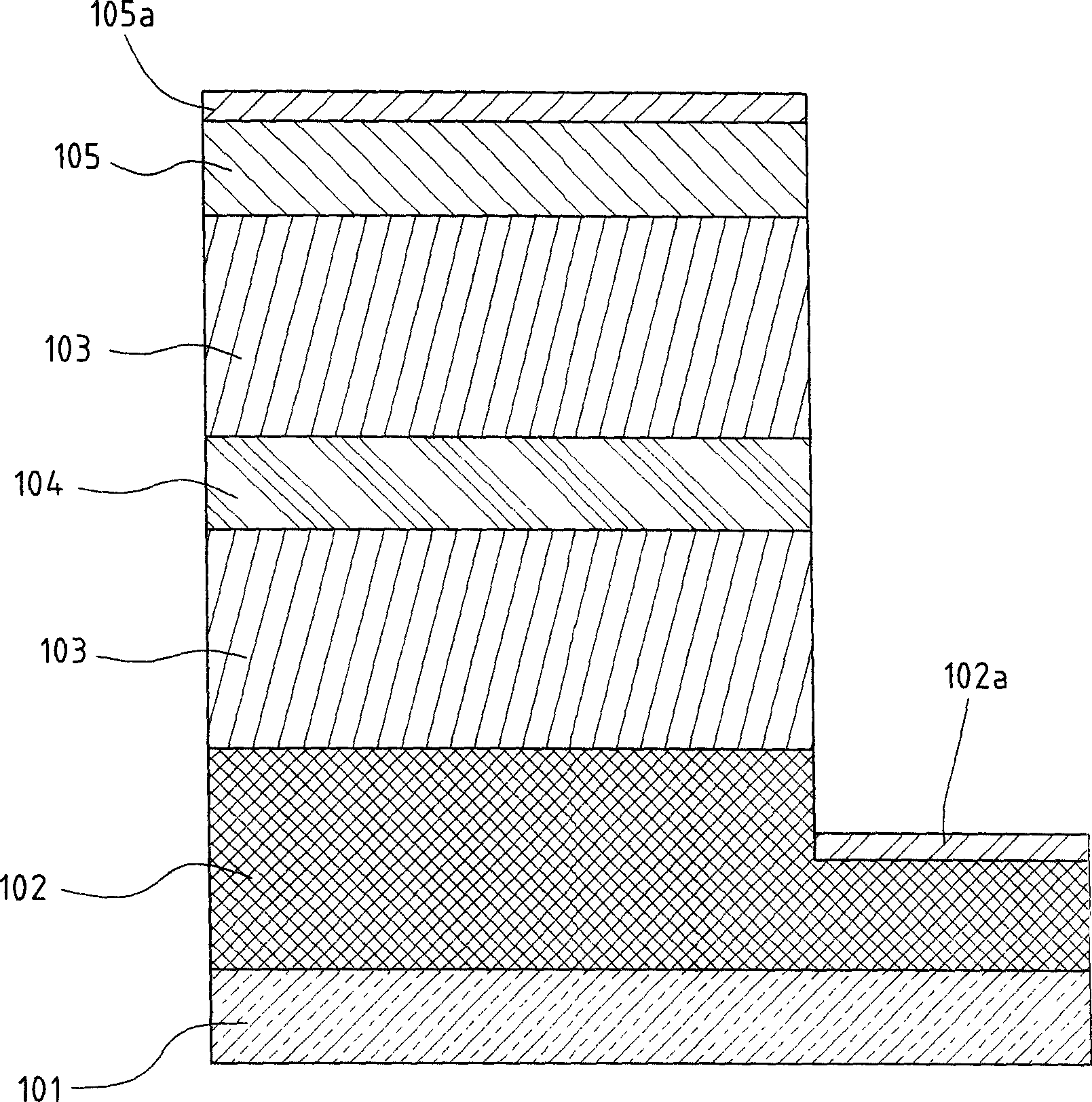
[0015] refer to figure 1 As shown, the first embodiment of the LED structure of the present invention includes: a substrate 101 , an N-type contact layer 102 , a barrier layer 103 , a light-emitting layer 104 and a P-type contact layer 105 .

[0016] The substrate 101 can be made of C-Plane or R-Plane or A-Plane alumina single crystal (Sapphire), or made of SiC (6H-SiC or 4H-SiC), Si, ZnO, GaAs or spinel Stone (MgAl 2 o 4 ), or a single crystal oxide whose lattice constant is close to that of a nitride semiconductor, in which Sapphire or SiC is generally used to form an N-type contact layer 102 on the substrate 101 . In addition, the N-type contact layer 102 is formed of N-type gallium nitride (GaN) material, an N-electrode layer 102 a in ohmic contact is formed on one side, and a barrier layer 103 is formed on the upper side.

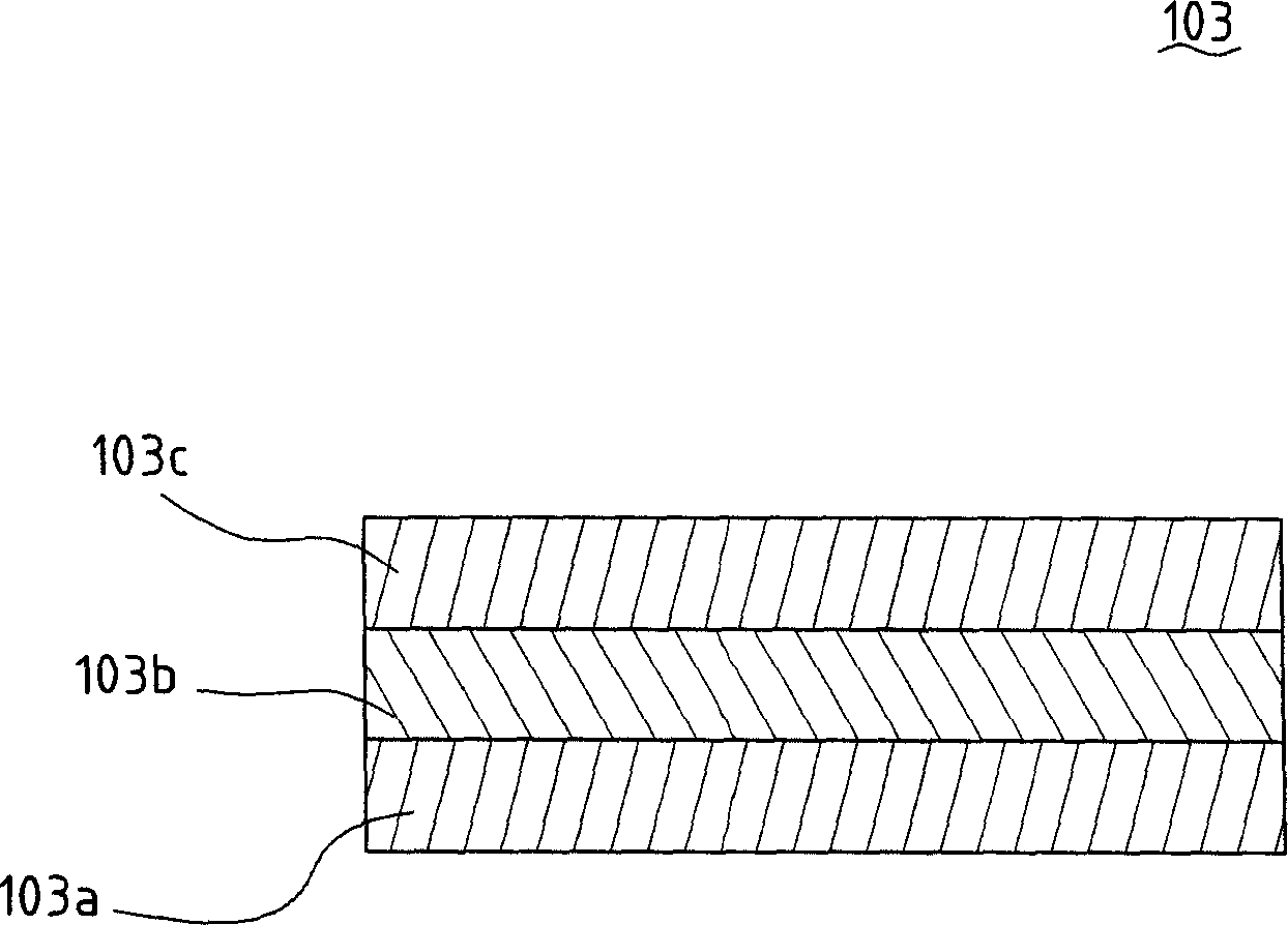
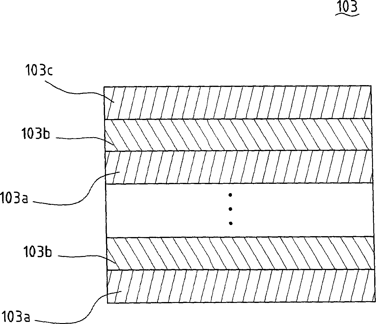
[0017] refer to figure 2 As shown, the barrier layer 103 includes: a first AlInGaN layer 103a, which is grown on the N-type contact layer 102 wi...


PUM


Abstract

The invention features a stacking structure on a baseboard of N type contact layer made of GaN material. It includes: a barrier layer stacked on the N type contact layer, in which an Alj-x GaxInyN layer, a SiN layer and another Alj-x GaxInyN layer are stacked in turn; a luminous layer that is an Alj-x GaxInyN layer formed on the barrier layer; another barrier layer; a SiN layer; an Alj-x GaxInyN layer; a P type contact layer located on top layer of barrier layer and made of Mg-doped P type GaN material; and a ohmic contact P type electrode layer is formed on its top; an ohmic contact N type electrode layer is formed at one side of N type contact layer above.

Description

technical field [0001] The present invention relates to a light emitting diode structure, and in particular provides a light emitting diode structure having a barrier layer and a light emitting layer. Background technique [0002] Traditional gallium nitride (GaN)-based light-emitting diode structure, the light-emitting layer mainly uses silicon (Si) doped gallium nitride as the barrier of multiple quantum wells to confine electron-hole pairs in the potential of indium gallium nitride (InGaN) The well combination is used to improve the internal quantum efficiency (internal quantum efficiency) and reduce the operating voltage of the device. However, part of the photons are absorbed by the silicon-doped GaN barrier and cannot escape from the entire multiple quantum well structure, which reduces the external quantum efficiency. In addition, V-type defects are also generated due to the increase in the stress of the multiple quantum well structure caused by the piezoelectric fie...

Claims


Application Information

Patent Timeline
IPC IPC(8): H01L33/00H01L33/04
Inventor 游正璋涂如钦武良文温子稷简奉任
Owner FORMOSA EPITAXY INCORPORATION
Why Eureka
Try Eureka