Auxiliary laser crystallization method for making polysilicon

An auxiliary laser and polysilicon technology, applied in semiconductor/solid-state device manufacturing, electrical components, circuits, etc., can solve the problems of small laser operation energy process window, increased production cost, unstable energy output, etc., and achieve good laser crystallization quality, Improve the uniformity of distribution and improve the electrical performance

Inactive Publication Date: 2006-05-10
IND TECH RES INST
View PDF0 Cites 5 Cited by
  • Summary
  • Abstract
  • Description
  • Claims
  • Application Information

AI Technical Summary

Problems solved by technology

However, the crystal grains of polysilicon formed by the above-mentioned solid phase crystallization method or direct vapor deposition method are quite small, with a particle size of only about 100nm. Therefore, the properties of polysilicon thin films formed by these methods are not good.
[0005] At present, the Excimer Laser Anneal (ELA) technology is most commonly used in the production of polysilicon thin films. Although the polysilicon grain size that can be obtained can reach about 600nm, for the development of higher performance planar The display is still not enough
Moreover, the general excimer laser tempering technology must use a high repetition rate irradiation method to improve the shortcomings of the excimer laser's uneven laser energy distributi...

Method used


Image

  • Auxiliary laser crystallization method for making polysilicon
  • Auxiliary laser crystallization method for making polysilicon
  • Auxiliary laser crystallization method for making polysilicon

Examples


Embodiment 1

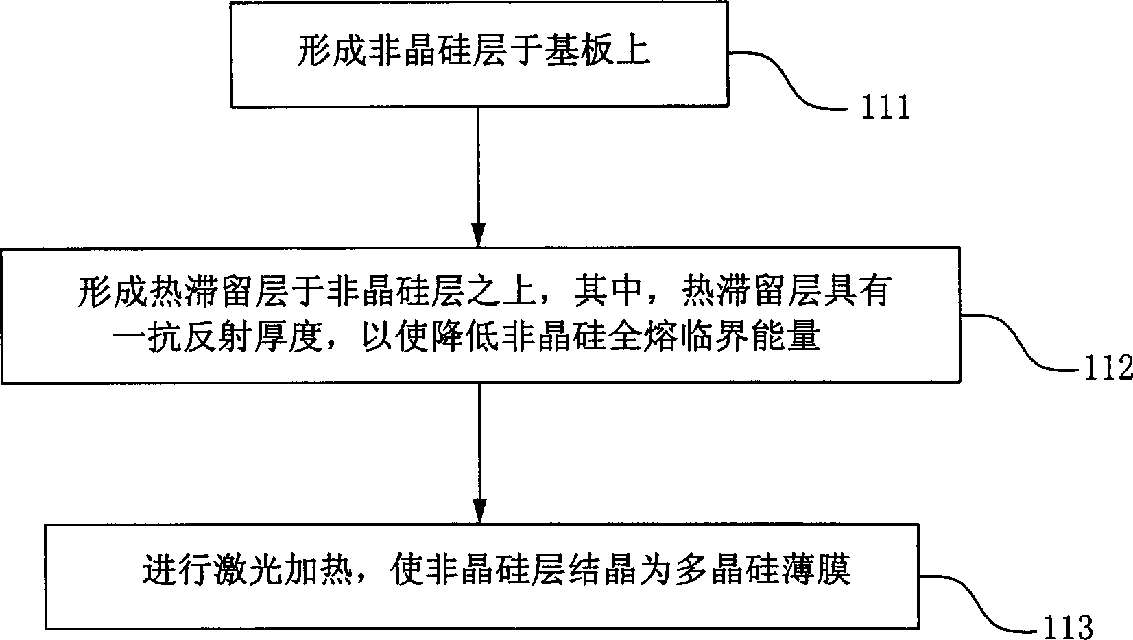
[0025] The invention discloses a method for assisting laser crystallization in polysilicon production. In the laser crystallization process of the amorphous silicon layer, in order to prolong the melting time of the amorphous silicon layer, a film material with semi-transparent properties can be selected as a heat retention layer to cover the amorphous silicon layer to be crystallized . In this way, when the laser light source is irradiated, in addition to part of the laser light source directly penetrating the amorphous silicon, there is also a part of the laser light source that can be absorbed by the heat retention layer, which has an additional heating effect on the amorphous silicon, thereby prolonging the cooling of the molten silicon. The time is in favor of the growth of large-sized crystal grains.

[0026] However, generally, the thermal stagnation layer with translucent properties also has partial light reflection properties at the same time, so the operating laser ...

Embodiment 2

[0037] The present invention also discloses another method of assisted laser crystallization applied to the production of polysilicon, which uses two heat retention layers that also have the effect of heat retention to cover the amorphous silicon. Control to achieve the anti-reflection effect on the laser light source. On the one hand, through the selection of the material of the thermal stagnation layer, the thermal stagnation layer has appropriate electrical properties for the fabrication of the thin film transistor element structure.

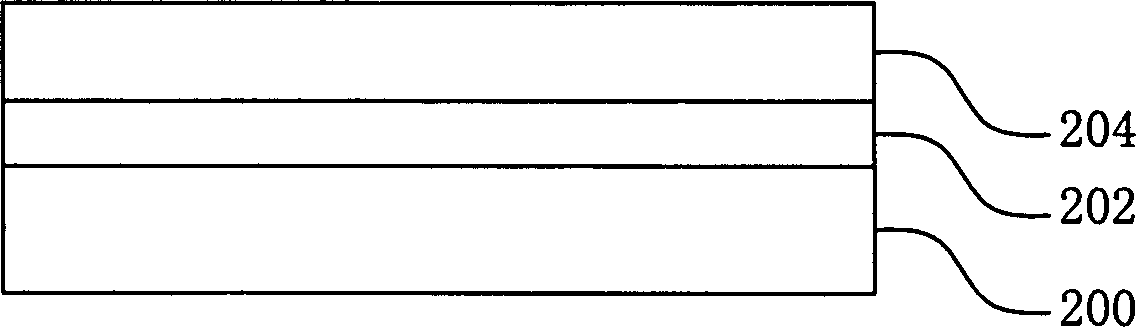
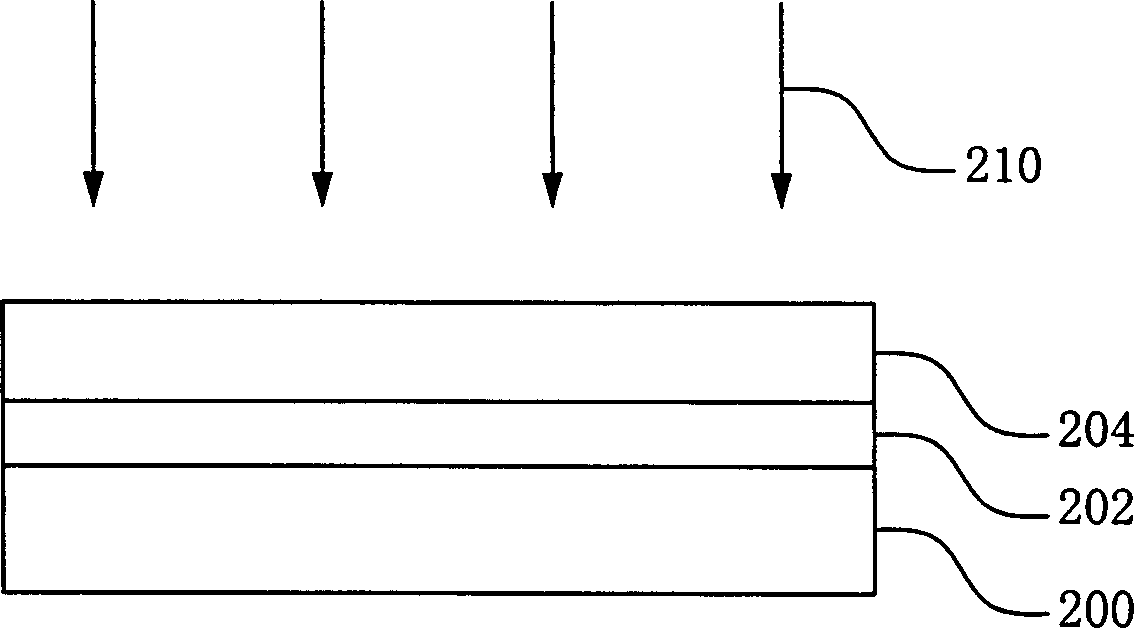
[0038] refer to Figures 4A-4B , Figures 4A-4B It is a schematic cross-sectional view of a method for assisting laser crystallization according to the second preferred embodiment of the present invention. First, refer to Figure 4A , to first form an amorphous silicon layer 402 on a substrate 400, wherein the amorphous silicon layer 402 is formed by, for example, plasma-assisted chemical vapor deposition or physical vapor deposition. In a...


PUM


Abstract

This invention relates to assistant laser crystal method, which comprises the following steps: forming non-crystal silicon layer on baseboard; then forming one thermal band in the non-crystal silicon layer, wherein, by control of thickness of the band, the band has one reflection thickness to lower non-crystal silicon melt threshold energy; Finally processing laser heating and crystal process to make the non-crystal into multi-crystal, wherein, the part laser energy passes thermal band to melt non-crystal layer with part laser energy in the ban to heat up non-crystal layer.

Description

technical field [0001] The present invention relates to a method for assisting laser crystallization, and in particular to a method for assisting laser crystallization which is applied to the production of polysilicon and has thermal retention characteristics and anti-reflection capabilities. Background technique [0002] Poly-silicon (poly-silicon) has been widely valued in the manufacture of thin-film transistors in recent years because of its electrical characteristics superior to amorphous silicon and cost considerations lower than that of single-crystal silicon, especially in thin-film transistors driving liquid crystal displays. (TFT-LCD) applications. [0003] However, the grain size of polysilicon crystals has a great influence on electron mobility and device characteristics. Among them, the grain-boundary existing in polysilicon is more constitutive of the carrier passing through the gate in the device. Obstacles in extreme passage. Therefore, how to increase the ...

Claims


Application Information

Patent Timeline
IPC IPC(8): H01L21/20H01L21/00H01L21/324
Inventor 林家兴陈麒麟陈昱丞蔡柏豪
Owner IND TECH RES INST
Why Eureka
Try Eureka