Method for detecting defect of single crystal structure of gallium arsenide in large size

A single crystal structure and defect detection technology, which is applied in the direction of optical testing flaws/defects, preparation of test samples, etc., can solve the problems of reducing measurement points, affecting measurement accuracy, and detection accuracy can not meet the requirements, etc., reaching the range of crystal orientation Expansion, short heating time, accurate detection effect

Inactive Publication Date: 2006-07-05
CHINA ELECTRONICS TECH GRP NO 46 RES INST
View PDF0 Cites 17 Cited by
  • Summary
  • Abstract
  • Description
  • Claims
  • Application Information

AI Technical Summary

Problems solved by technology

[0004] At present, the steps of the existing method for detecting the dislocation density of GaAs single crystal are as follows: grinding, polishing, etching, testing and calculating the cut GaAs single wafer. When etching the wafer, it needs to be heated by potassium hydroxide The sample can only be corroded when the temperature is 400°±5°C, which requires a thermometer to measure, so that the corrosion time of a large-scale gallium arsenide single wafer is controlled by the existing method, and the corrosion effect is not clear, not ideal, or even uncountable It will bring a large detection error, which directly affects the measurement accuracy, and also

Method used


Image

  • Method for detecting defect of single crystal structure of gallium arsenide in large size
  • Method for detecting defect of single crystal structure of gallium arsenide in large size
  • Method for detecting defect of single crystal structure of gallium arsenide in large size

Examples


Embodiment 1

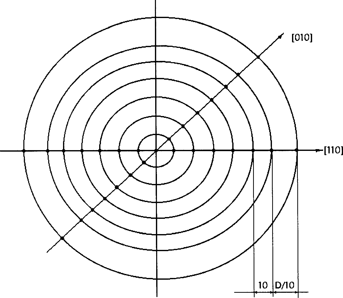
[0033] Embodiment 1, the detection steps of the dislocation defect of 150mm gallium arsenide are as follows:

[0034] (1) Grinding, grinding the cut 150mm gallium arsenide single wafer with emery to make the surface smooth, smooth and scratch-free, and cleaning;

[0035] (2) Polishing: chemical polishing is adopted, and the formula of the polishing liquid is sulfuric acid: hydrogen peroxide: water = 3: 1: 1. When polishing a crystal orientation single crystal, it is necessary to stir the prepared polishing liquid and place it at room temperature, and then put Immerse the single crystal in the polishing solution until the single crystal is polished, and the temperature of the polishing solution does not need to reach room temperature when polishing other single crystals;

[0036](3) Dislocation corrosion, put potassium hydroxide in a silver crucible and heat it, and when the potassium hydroxide is melted and heated to a clear state, put it into the wafer sample for corrosion...

Embodiment 2

[0048] Example 2 Detection of Dislocation Density on Gallium Arsenide Single Wafer with a Size of 180 mm

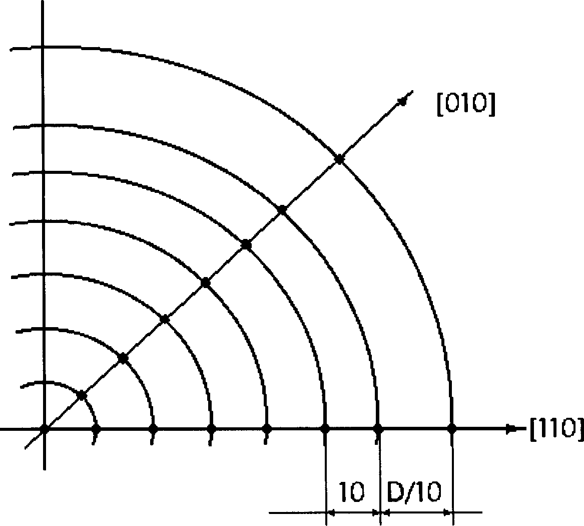
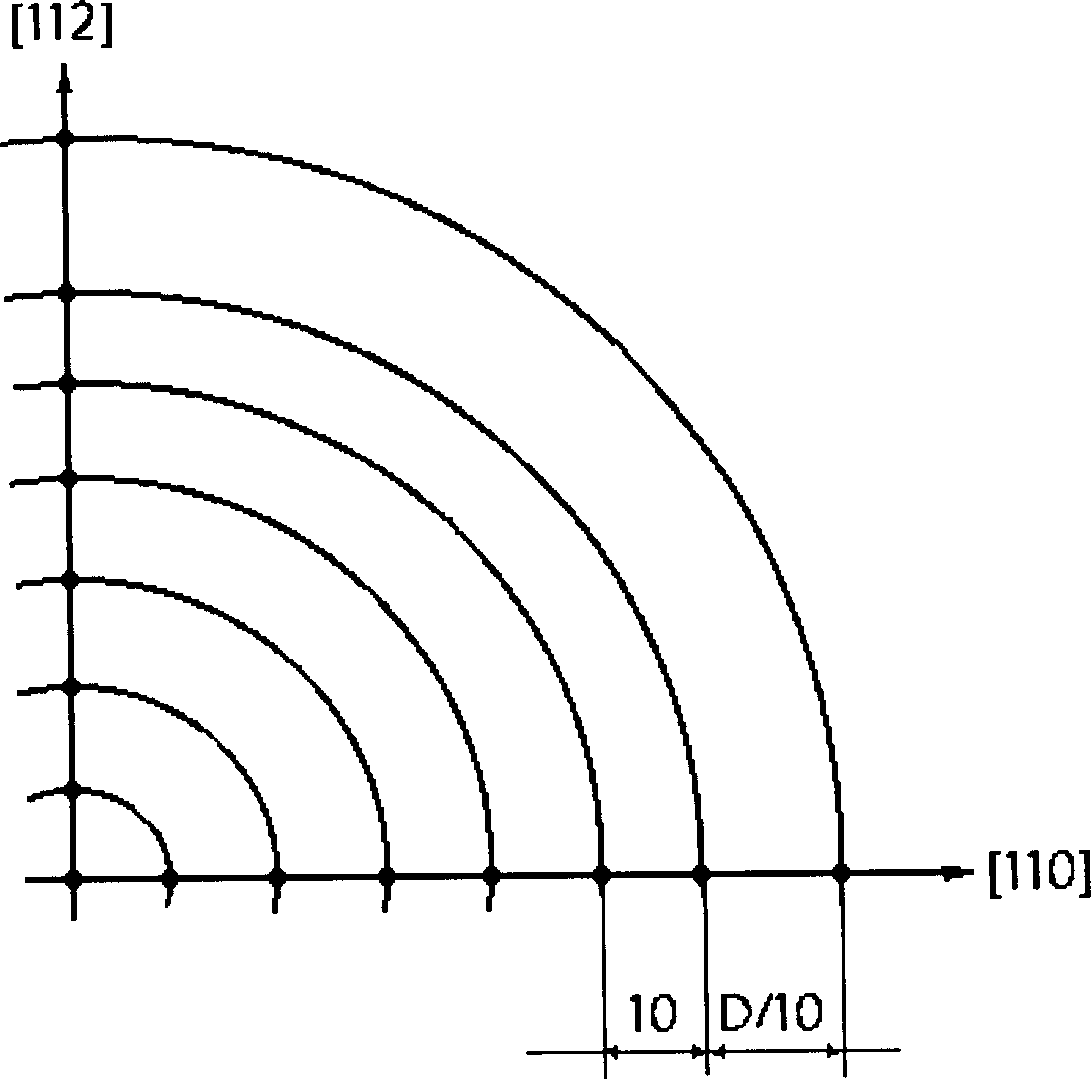
[0049] The whole implementation steps are the same as the 150mm diameter gallium arsenide single wafer, except that the selection of the detection field position is different, that is, the mask preparation is different. The first measurement point is selected at D / 10mm from the edge of the wafer, which is 18mm. Every 12mm interval of measurement points is a measurement field of view, and the selection direction is the same, so that the number of measurement points is the same as that of a 150mm diameter single crystal, but the selected positions are different. Other grinding-polishing-corrosion-observation-calculation are the same.


PUM


Abstract

The invention is a defect detecting method for a large-size GaAs monocrystalline structure, comprising: grinding and polishing, i.e. mechanically or chemically polishing, where the formula of the adopted polishing solution is that the ratio of sulphuric acid to oxydol to water is 3 : 1 : 1; dislocation corroding, i.e. placing potassium hydroxide in a silver pot and heating to melt potassium hydroxide into a clear state and immediately placing the clear-state potassium hydroxide in a wafer sample for corroding, then taking out the sample and cooling, and then washing with water and blow-dry; selecting measuring direction, measuring point position and number of measuring points, observing visual field area, where the first measuring point is D/10mm apart from the wafer edge and the others are selected at 10 mm intervals, each of which is a measuring visual field; calculating for the selected measuring points. The invention enlarges the range of dislocation density detection, convenient and simple to operate and saving time.

Description

[0001] Field [0002] The invention relates to a method for detecting structural defects of gallium arsenide single crystals applied in the field of semiconductors, in particular to a method for detecting dislocation density of large-scale gallium arsenide single crystals. Background technique [0003] Dislocations are revealed using selective chemical etching techniques. The lattice around the dislocation lines in the crystal is distorted, and the outcrops on the crystal surface are preferentially corroded by certain chemical etchants. Therefore, it is easy to form an angular corrosion pit or hillock with a specific shape composed of some low-index surfaces at the outcrop of defects on a certain crystal surface of the crystal. [0004] At present, the steps of the existing method for detecting the dislocation density of GaAs single crystal are as follows: grinding, polishing, etching, testing and calculating the cut GaAs single wafer. When etching the wafer, it needs to be h...

Claims


Application Information

Patent Timeline
IPC IPC(8): G01N1/32G01N21/88
Inventor 周智慧章安辉王香泉
Owner CHINA ELECTRONICS TECH GRP NO 46 RES INST
Why Eureka
Try Eureka