Low temperature airtightness packaging method for wafer level micro machinery device and photoelectric device

A technology for micromechanical devices and optoelectronic devices, applied in metal processing mechanical parts, optomechanical equipment, microstructure devices, etc., can solve the problems of heavy metal pollution in CMOS circuits, difficulty in obtaining large-area bonding, and high bonding temperature of hard solders. Achieve the effect of reducing residual thermal stress, improving process compatibility and good bonding performance

Inactive Publication Date: 2006-08-23
QST CORP
View PDF0 Cites 14 Cited by
  • Summary
  • Abstract
  • Description
  • Claims
  • Application Information

AI Technical Summary

Problems solved by technology

But gold may cause heavy metal contamination of CMOS circuits, which is not desirable
Gold-silicon eutectic bonding also has major drawbacks: it is difficult to obtain complete large-area bonding, and the presence of native oxides also prevents bonding
The two solders have their own advantages and disadvantages, that is, the hard solder has a high bonding temperature, can be used at high temperatures, and has high strength; but after cooling, the residual thermal stress is large

Method used


Image

  • Low temperature airtightness packaging method for wafer level micro machinery device and photoelectric device
  • Low temperature airtightness packaging method for wafer level micro machinery device and photoelectric device
  • Low temperature airtightness packaging method for wafer level micro machinery device and photoelectric device

Examples


Embodiment 1:MEMS( and other approach ), specific pic 5。 Embodiment approach

[0071] Embodiment 1: Carry out low-temperature wafer-level airtight packaging to resonant MEMS devices (comprising resonant beam type and other modes of resonant devices), the specific process flow is as follows Figure 5 shown. The implementation method is as follows:

[0072] (1) Select a semiconductor material such as silicon wafer 1 (ordinary N-type (100) double-polished silicon wafer, thickness 420±15 μm, resistivity 3-8 (Ω cm)), and oxidize to obtain the top mask silicon dioxide 2 and underlying silica 3, such as Figure 5 (b).

[0073] (2) apply photoresist 4 (in this experiment, adopt the trade mark 1912 type photoresist of Shipley Company), and pattern exposure, development, obtain such as Figure 5 (d) structure, forming a mask for the opening of the top layer of silicon dioxide 2 .

[0074] (3) corrode top layer mask silicon dioxide 2 in BOE etching solution, open etching window for it, remove photoresist 4 subsequently, as Figure 5 (f).

[0075] (4) In KOH o...

Embodiment 2

[0079] Embodiment 2: low-temperature wafer-level airtight packaging is carried out to micro-accelerometer devices (comprising small-range high-precision accelerometers, high-range accelerometers, micro-accelerometers moving in the vertical direction, and horizontally sliding micro-accelerometers), specifically The implementation method refers to steps (1) to (7) in Example 1, except that the resonant micromechanical movable part in the cavity is replaced by the micro accelerometer movable part 7 .

Embodiment 3

[0080] Embodiment 3: Carry out low-temperature wafer-level hermetic packaging of micro-gyro devices (including micro-gyro devices such as micro-mechanical capacitive and piezo-resistive types), and the specific implementation method refers to the steps in embodiment 1: (1)~(7) , just replace the resonant micromechanical movable part in the cavity with the microgyro movable part 7 .


PUM

PropertyMeasurementUnit
thicknessaaaaaaaaaa
electrical resistivityaaaaaaaaaa
thicknessaaaaaaaaaa

Abstract

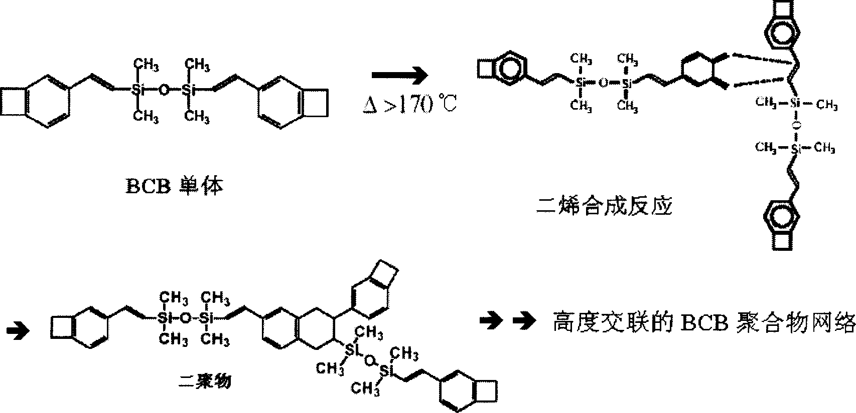
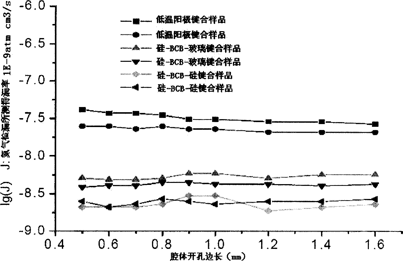
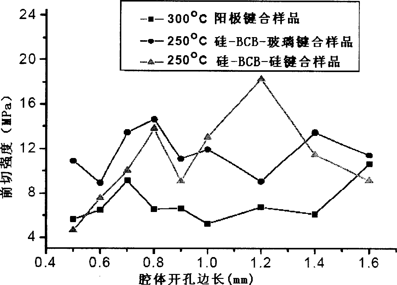
The low temperature airtight packaging method for wafer level micro mechanical device and photoelectric device features that semiconductor material or glass through wet etching or dry etching is airtight bonded at pressure of (1-3)í‡10<-5> Pa and vacuum degree of 10< -3 > Pa by using benzocyclobutene (BCB). The BCB bonded micro mechanical device and photoelectric device may reach air tightness of (2.1í½5.9)í‡10< -4 > Pa cu cm / s He and shear strength over 4.65 MPa. The packaging method of the present invention is suitable for MEMS device, micro acceleration meter, micro gyro, micro heat radiation instrument, etc. and can raise the performance of the packaged device obviously.

Description

technical field [0001] The invention relates to a low-temperature hermetic packaging method for wafer-level micromechanical devices and photoelectric devices, in particular, a method for using benzocyclobutene (BCB) materials for wet-etching or dry-etching Low-temperature wafer-level hermetic bonding of semiconductor materials or glass to achieve low-temperature wafer-level hermetic packaging of micromechanical devices and optoelectronic devices. The invention belongs to the technical fields of micromechanical devices, photoelectric devices and microfabrication. Background technique [0002] Some MEMS (micro-electro-mechanical systems) devices are easily damaged during the scribing and assembly process due to their structure containing some movable parts; at the same time, they are exposed to dust, airflow, water vapor, mechanical impurities and other substances in the working environment for a long time It also affects the service life of the device. These special-purpose...

Claims


Application Information

Patent Timeline
Patent Type & Authority Applications(China)
IPC IPC(8): B81C3/00B81C1/00
Inventor 刘玉菲吴亚明李四华刘文平
Owner QST CORP
Why Eureka
Try Eureka