Method of processing and cleaning substrate, and method of and program for manufacturing electronic device

A substrate processing method and technology of the processing method are applied in the manufacturing field of electronic equipment, and can solve the problems of easy dissolving of surface damage layer and cutting residue by cleaning liquid, and difficulty in controlling the removal amount of surface damage layer and cutting residue.

Inactive Publication Date: 2006-08-23
TOKYO ELECTRON LTD
View PDF1 Cites 6 Cited by
  • Summary
  • Abstract
  • Description
  • Claims
  • Application Information

AI Technical Summary

Problems solved by technology

[0013] However, the above-mentioned cleaning step is equivalent to a wet etching step using a chemical solution. In the cleaning step, the cleaning solution easily dissolves

Method used


Image

  • Method of processing and cleaning substrate, and method of and program for manufacturing electronic device
  • Method of processing and cleaning substrate, and method of and program for manufacturing electronic device
  • Method of processing and cleaning substrate, and method of and program for manufacturing electronic device

Examples


Embodiment Construction

[0105] Embodiments of the present invention will be described below with reference to the drawings.

[0106] First, a substrate processing method according to an embodiment of the present invention will be described.

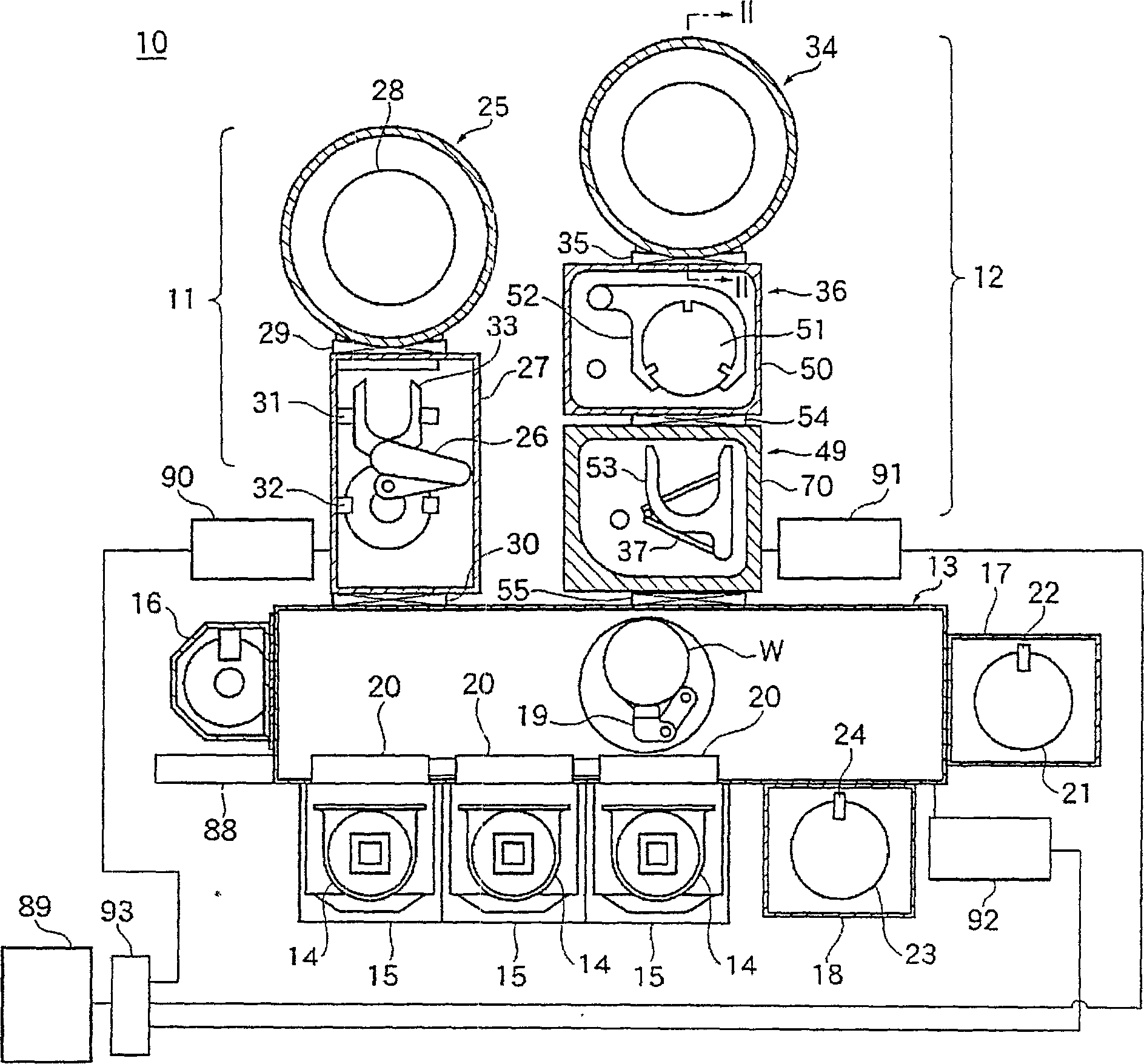
[0107] figure 1 It is a plan view showing a schematic configuration of a substrate processing apparatus to which the substrate processing method of this embodiment is applied.

[0108] exist figure 1 Among them, the substrate processing apparatus 10 has a first processing chamber 11 for performing reactive ion etching (hereinafter referred to as "RIE") on a wafer (hereinafter referred to as "wafer") (substrate) W for electronic equipment; The processing cabin 11 is arranged in parallel, and carries out the second processing cabin 12 of the COR (chemical oxide removal Chemical Oxide Removal) process and PHT (Post Heat Treatment Post Heat Treatment) described later on the wafer W; A rectangular common transfer chamber loading unit 13 connected to the second p...


PUM


Abstract

A method of processing a substrate which enables a surface damaged layer and polishing remnants on the surface of an insulating film to be removed, and enable the amount removed of the surface damaged layer and polishing remnants to be controlled easily. An insulating film on a substrate, which has been revealed by chemical mechanical polishing, is exposed to an atmosphere of a mixed gas containing ammonia and hydrogen fluoride under a predetermined pressure. The insulating film which has been exposed to the atmosphere of the mixed gas is heated to a predetermined temperature.

Description

technical field [0001] The present invention relates to the processing method of substrate, the cleaning method after chemical mechanical polishing, the manufacturing method and program of electronic equipment; Particularly relate to after utilizing chemical mechanical polishing to grind the conductive film that forms on the surface, by carrying out plasma-less etching (plasma-less etching) processing, a method of manufacturing electronic devices that improves surface flatness. Background technique [0002] In an electronic device manufacturing method for manufacturing an electronic device composed of a silicon wafer (hereinafter referred to as "wafer"), the process of forming a photoresist layer with a desired pattern on an insulating film formed on the surface of the wafer is repeated sequentially. Photolithography process; using the photoresist layer as a mask, using plasma to form a conductive film on the gate electrode, or an etching process to form wiring grooves or co...

Claims


Application Information

Patent Timeline
IPC IPC(8): H01L21/3105H01L21/768
Inventor 西村荣一岩﨑贤也
Owner TOKYO ELECTRON LTD
Why Eureka
Try Eureka