Growing method of indium arsenide nano-ring prepared by indium arsenide-indium alluminum arsenide laminate point

A growth method and technology of indium arsenide, which are applied in the directions of nanotechnology, nanotechnology, nanostructure manufacturing, etc., to achieve the effects of simple method, high efficiency and improved areal density

Inactive Publication Date: 2006-09-13
INST OF SEMICONDUCTORS - CHINESE ACAD OF SCI
View PDF0 Cites 1 Cited by
  • Summary
  • Abstract
  • Description
  • Claims
  • Application Information

AI Technical Summary

Problems solved by technology

The method that the present invention proposes to grow indium aluminum arsenic (InAlAs) nano-quantum dots and then wrap them with InAs has no reports at home and abroad

Method used


Image

  • Growing method of indium arsenide nano-ring prepared by indium arsenide-indium alluminum arsenide laminate point
  • Growing method of indium arsenide nano-ring prepared by indium arsenide-indium alluminum arsenide laminate point

Examples


example

[0030] combined reference figure 1 and figure 2 :

[0031] (1) realize main equipment of the present invention

[0032] Molecular Beam Epitaxy System

[0033] Mechanical vacuum pump + diffusion vacuum pump (or other vacuum equipment)

[0034] temperature control system

[0035] According to the specific conditions of the growth equipment, make appropriate adjustments to the growth technology route.

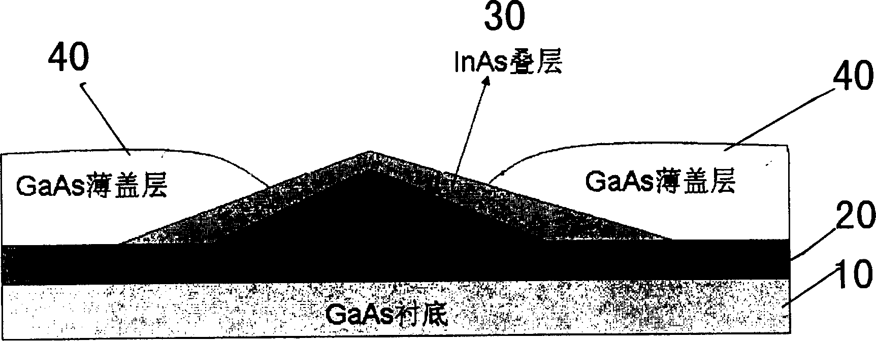
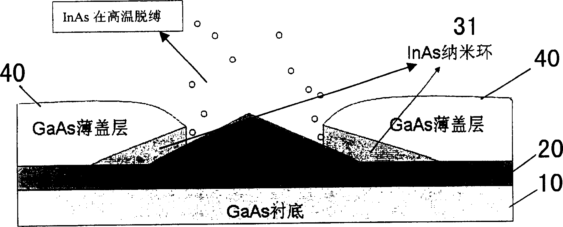
[0036] (2) using a semi-insulating GaAs (001) single crystal as the substrate 10;

[0037] (3) Using a molecular beam epitaxy system to epitaxially grow a 200nm GaAs buffer layer on the GaAs substrate 10 (not shown in the figure, the buffer layer may not be present);

[0038] (4) At a temperature of 550°C, 5.6×10 -6 Torr's As 2 Heteroepitaxial growth of 10 molecular monolayer (ML) InAlAs layers 20 in the atmosphere, and the formation of self-assembled quantum dots was observed by the high-energy electron diffraction system;

[0039] (5) epitaxially growing a molecular si...


PUM

PropertyMeasurementUnit
thicknessaaaaaaaaaa

Abstract

This invention relates to a method for preparing InAs nm rings by InAs-InAlAs lamination points characterizing the following steps: 1, taking a semi-insulated GaAs mono-crystal chip as the substrate, 2, epitaxially growing InAlAs layer for heterogeneity on the substrate, 3, epitaxially growing InAs lamination layer on said InAlAs layer, 4, epitaxially growing a GaAs thin cover layer on the InAs lamination layer, 5, annealing and taking away the InAs lamination layer to finish the growing of InAs nm rings.

Description

technical field [0001] The invention provides a growth method of an indium arsenide (InAs) ring nanostructure on a gallium arsenide (GaAs) substrate, in particular a growth method of partially covering InAlAs nano dots wrapped by InAs and annealing at high temperature. Background technique [0002] Semiconductor materials and nanomaterials are two key and hot areas of current materials science. Combining the quantum properties of nanomaterials with the energy band properties of semiconductor materials is a very important branch of semiconductor physics and an important way to manufacture new functional devices. The performance of optoelectronic devices made of low-dimensional semiconductor heterojunction materials, such as lasers and detectors, has been rapidly improved, and they have quickly entered the market and been widely used. Therefore, the preparation of nano-semiconductor materials is of great significance to both material science and practical applications. [00...

Claims


Application Information

Patent Timeline
Patent Type & Authority Applications(China)
IPC IPC(8): H01L21/00H01L31/18H01S5/00B82B3/00
CPCY02P70/50
Inventor 李凯叶小玲王占国
Owner INST OF SEMICONDUCTORS - CHINESE ACAD OF SCI
Why Eureka
Try Eureka