Electrophotographic photoreceptor for blue-violet exposure light source and electrophotographic imaging apparatus employing the same
An electrophotography and imaging device technology, applied in the electrical recording process using charge patterns, equipment, optics, etc., can solve the problems of reduced light absorption, reduced light energy, and insufficient photosensitivity. achieve high resolution
- Summary
- Abstract
- Description
- Claims
- Application Information
AI Technical Summary
Problems solved by technology
Method used
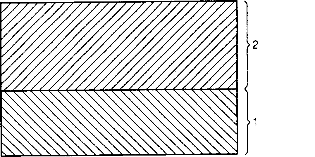
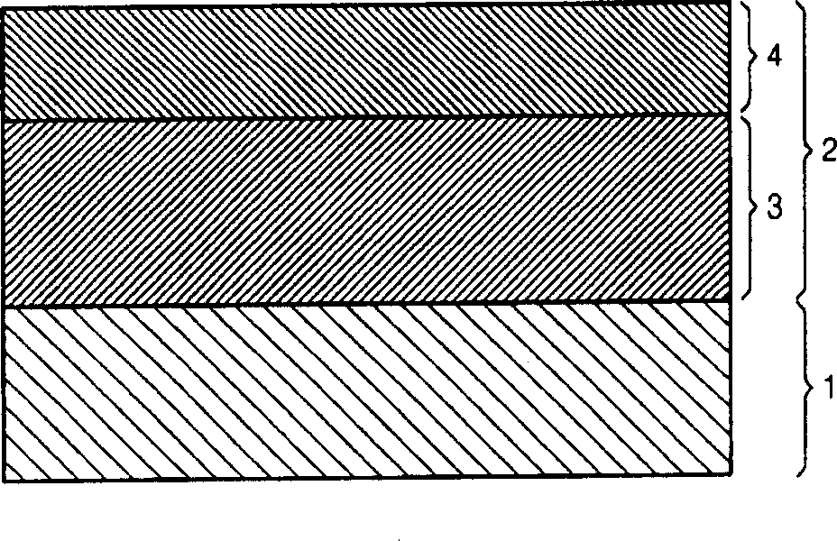
Image

Examples
Embodiment 1
[0059] 2 parts by weight of α-titanyl phthalocyanine and 2 parts by weight of polycarbonate Z resin (PANLITETS-2020, Teijin Kasei Co.) were mixed with 46 parts by weight of chlorobenzene. The mixture was ground with a sand mill for 1 hour to finely disperse it.
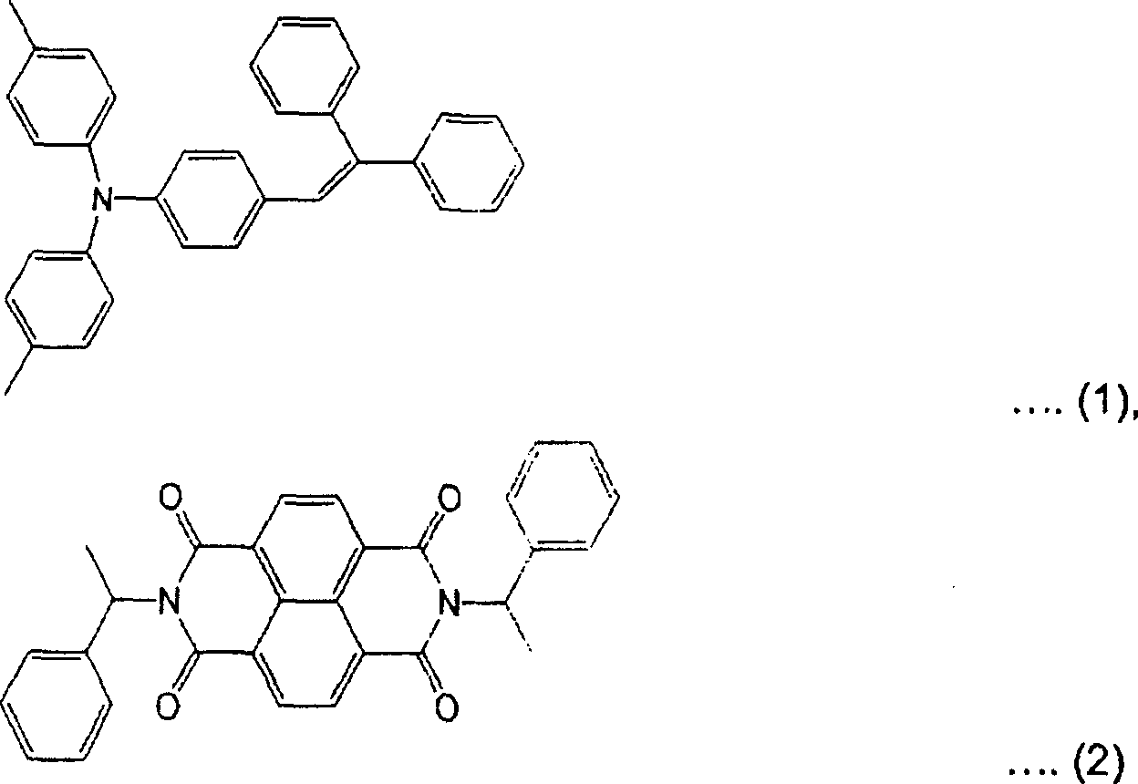
[0060]35 parts by weight of the compound (1) based on arylamine as the hole transport material, 15 parts by weight of the compound (2) based on naphthalene tetracarboxylic acid diimide and 50 parts by weight of polycarbonate as the electron transport material Ester Z resin was dissolved in 300 parts by weight of chloroform.
[0061]
[0062] The dispersed substance and the solution were mixed in a weight ratio of 1:8. The mixture was dispersed homogeneously with a homogenizer, thereby obtaining a coating slurry for forming a photosensitive layer. The coating slurry was coated onto a 30 nm diameter anodized aluminum drum (anodized layer thickness: 5 μm) with a ring bar, and then dried, whereby a single-layer elect...
Embodiment 2
[0064] A photoreceptor drum was produced in the same manner as in Example 1 except that the weight ratio of the dispersed substance and the solution was 1:4. The transmittance measured at a wavelength of 405nm is 5.5×10 -2 .
Embodiment 3
[0066] 40 parts by weight of arylamine-based compound (1), 60 parts by weight of polycarbonate Z resin as a hole transport material were dissolved in 300 parts by weight of chloroform, thereby obtaining a solution for forming a charge transport layer . The solution was applied onto a 30 mm diameter anodized aluminum drum (anodized layer thickness: 5 μm) using a ring bar, and then dried, whereby a charge transport layer having a thickness of about 8 μm was obtained.
[0067] The dispersed substance and solution used in Example 1 were mixed at a weight ratio of 1:2, whereby a dispersion for forming a charge generating layer was obtained. Next, this dispersion was applied onto the charge transport layer using a ring bar, followed by drying, whereby a charge generation layer having a thickness of about 7 μm was obtained.
[0068] The light transmittance at a wavelength of 405 nm of the obtained multilayer electrophotographic photoreceptor drum was 8.9×10 -2 .
PUM
 Abstract
Description
Claims
Application Information