High efficiency deep ultraviolet light-emitting diode

A light-emitting diode, deep ultraviolet technology, applied in electrical components, circuits, semiconductor devices, etc., can solve problems such as P-type conduction difficulties, and achieve the effects of increasing luminous efficiency, improving luminous efficiency, and improving reliability.

Inactive Publication Date: 2007-02-28
INST OF SEMICONDUCTORS - CHINESE ACAD OF SCI
View PDF0 Cites 20 Cited by
  • Summary
  • Abstract
  • Description
  • Claims
  • Application Information

AI Technical Summary

Problems solved by technology

Obviously, it is quite difficult to realize the P-type

Method used


Image

  • High efficiency deep ultraviolet light-emitting diode
  • High efficiency deep ultraviolet light-emitting diode
  • High efficiency deep ultraviolet light-emitting diode

Examples


Embodiment Construction

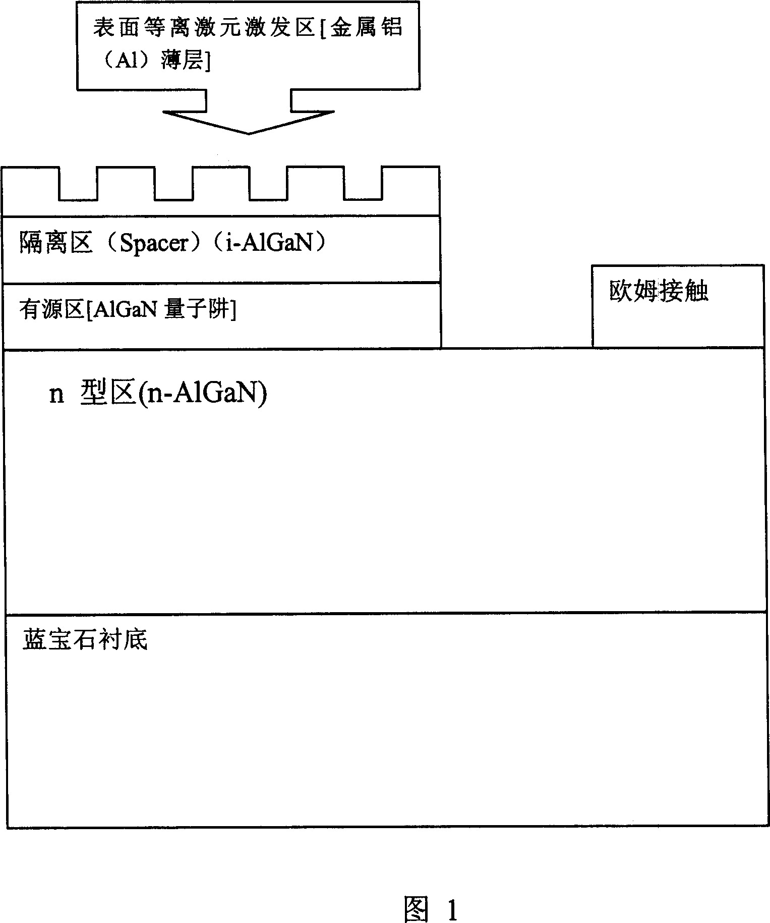
[0038] The specific implementation method of the preparation of the device structure in Figure 1: (taking AlGaN as an example)

[0039] 1) First grow n-type AlGaN several microns thick on the sapphire substrate;

[0040] 2) Then grow the intrinsic quantum well active region on it, (such as Al 0.8 Ga 0.2 N / Al 0.18 Ga 0.82 N multiple quantum wells);

[0041] 3) On the multiple quantum wells, an intrinsic AlGaN isolation layer (spacer) with a thickness of several to tens of nanometers (nm) is grown. Electron recombination coupling to periodic structure electrodes to excite surface plasmons);

[0042] 4) Etching away a part of AlGaN and quantum well until the bottom n-AlGaN is exposed;

[0043] 5) making ohmic contact electrodes on the exposed n-AlGaN surface;

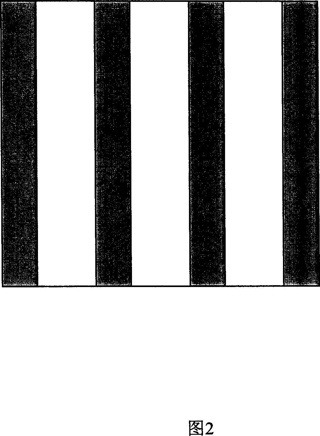
[0044] 6) On the surface of the remaining AlGaN isolation layer, use aluminum (Al) to make a grid-shaped electrode as shown in Figure 2 (it can also be a two-dimensional structure such as a ring, grid, and periodic is...


PUM


Abstract

The invention relates to a deep-ultraviolet light-emitting diode structure. Wherein, said structure uses plasma excimer effect; the surface plasma excimer is the oscillating wave formed by coupled optical field and carrier at the surface of conductor; the activation and couple of surface plasma excimer are realize by metal film with periodical structure; and the metal film has electrode contact function; and the metal part of common MIS light-emitting diode uses periodical structure generating surface plasma excimer.

Description

technical field [0001] The invention relates to the technical field of light-emitting diodes, in particular to a MIS (metal-insulator-semiconductor structure) deep ultraviolet (UV) light-emitting diode (LED) structure that utilizes the plasmon effect to improve the quantum efficiency of light emission. Background technique [0002] Deep ultraviolet (UV) light-emitting diodes (LEDs) are widely used in lighting, high-density optical storage, environmental treatment and detection, biology, and medicine. [0003] The most mature semiconductor materials used in deep ultraviolet light-emitting diodes are AlGaN (3.4-6.2ev) and AlInGaN (energy band range 0.7-6.2ev) systems, and the ZnMgO (energy band range 3.3-7.8ev) system is still in the development stage. These two materials (AlInGaN and AlGaN are actually a material system, collectively referred to as AlGaN hereinafter) both face the extremely difficult problem of P-type doping. The P-type doping of GaN materials is not easy. W...

Claims


Application Information

Patent Timeline
IPC IPC(8): H01L33/00
Inventor 康亭亭刘祥林
Owner INST OF SEMICONDUCTORS - CHINESE ACAD OF SCI
Why Eureka
Try Eureka