Novel tarc material for immersion watermark reduction and method for immersion watermark reduction

A technology of photoresist materials and lithography, which is applied in the direction of photosensitive materials used in photomechanical equipment, photosensitive material processing, microlithography exposure equipment, etc., can solve the problems of reducing the quality of semiconductor manufacturing, general products without structure, and errors. To achieve the effect of avoiding watermark defects

Active Publication Date: 2007-04-04
TAIWAN SEMICON MFG CO LTD
View PDF0 Cites 0 Cited by
  • Summary
  • Abstract
  • Description
  • Claims
  • Application Information

AI Technical Summary

Problems solved by technology

However, immersion lithography leaves water droplets after exposure
Residual water droplets will cause watermark defects, which will reduce the quality of semiconductor manufacturing and cause errors
[0003] It can be seen that the above-mentioned existing photoresist materials for immersion lithography and immersion lithography methods obviously still have inconveniences and defects in structu

Method used


Image

  • Novel tarc material for immersion watermark reduction and method for immersion watermark reduction
  • Novel tarc material for immersion watermark reduction and method for immersion watermark reduction
  • Novel tarc material for immersion watermark reduction and method for immersion watermark reduction

Examples


Embodiment Construction

[0053] In order to further explain the technical means and effects that the present invention adopts to achieve the intended purpose of the invention, the photoresist material for immersion lithography and the immersion lithography method proposed according to the present invention will be described below in conjunction with the accompanying drawings and preferred embodiments. Specific embodiments, structures, features and effects thereof are described in detail below.

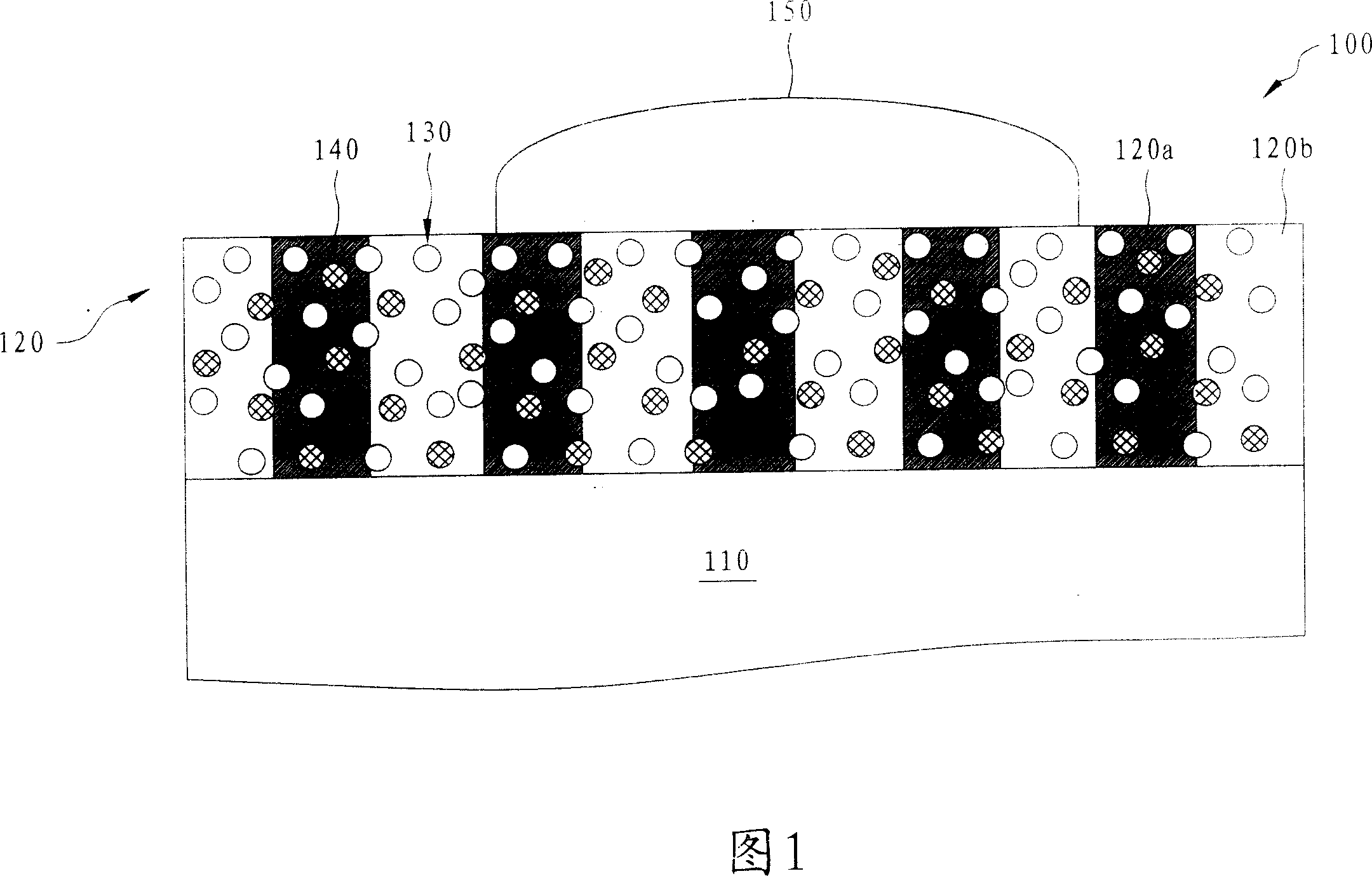
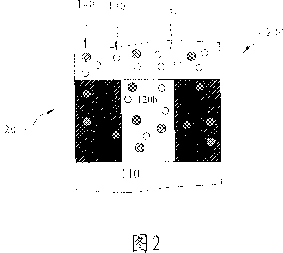
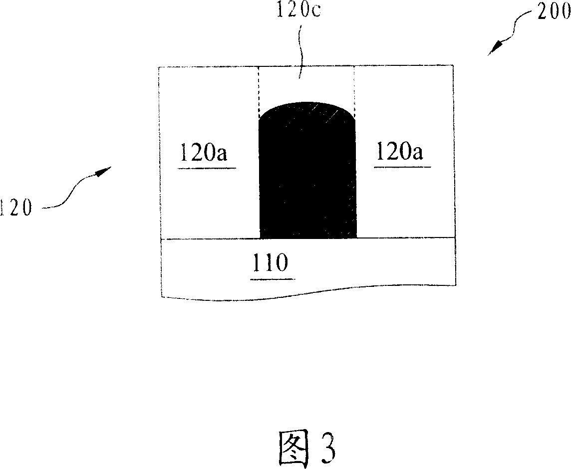
[0054] Please refer to FIG. 1 , which is a cross-sectional view of a semiconductor device 100 in an immersion lithography exposure process. The semiconductor device 100 may be a semiconductor wafer or other suitable devices. In this embodiment, the semiconductor device 100 includes a silicon substrate 110 and an organic bottom anti-reflective layer, an inorganic bottom anti-reflective layer, an organic etch stop layer, an organic adhesive layer, various doped layers, a dielectric layer and a multilayer Inline...


PUM


Abstract

A coating material disposed over a photosensitive layer comprises an acid capable of neutralizing a base quencher from the photosensitive layer; and a polymer that is a carrier of the acid and is insoluble to an immersion fluid used in an immersion lithography process. The acid is chemically bonded to the polymer or mixed to the polymer. The acid is an organic acid comprising a sulfonyl acid group. The polymer comprises fluoride. The coating material is soluble in tetramethylammonium hydroxide (TMAH) solution or cyclohexanol. An independent claim is included for a method for immersion lithography.

Description

technical field [0001] The invention relates to a photoresist material, in particular to an immersion lithography photoresist material and an immersion lithography method. Background technique [0002] In order to allow semiconductor manufacturing technology to continue to advance to a smaller size (such as 65 nanometers and below 45 nanometers), the latest semiconductor manufacturing technology uses immersion lithography technology. However, immersion lithography leaves water droplets after exposure. Residual water droplets will cause watermark defects, which will reduce the quality of semiconductor manufacturing and cause errors. [0003] It can be seen that the above-mentioned existing photoresist materials for immersion lithography and immersion lithography methods obviously still have inconveniences and defects in structure and use, and further improvement is urgently needed. In order to solve the above-mentioned problems, the relevant manufacturers have tried their b...

Claims


Application Information

Patent Timeline
IPC IPC(8): G03F7/004G03F7/20G03F7/26H01L21/027
CPCG03F7/11G03F7/2041G03F7/091Y10S430/111G02B1/111G03F7/09
Inventor 张庆裕
Owner TAIWAN SEMICON MFG CO LTD
Why Eureka
Try Eureka