

Nonvolatile semiconductor memory device
A storage device, non-volatile technology, applied in the direction of semiconductor devices, information storage, static memory, etc., can solve the problems of excessive erasure, increase of memory unit occupied area, conflict of processing size limit, etc., and achieve the goal of increasing data rewriting times Effect
- Summary
- Abstract
- Description
- Claims
- Application Information
AI Technical Summary
Problems solved by technology
Method used
Image

Examples
no. 1 Embodiment approach 》
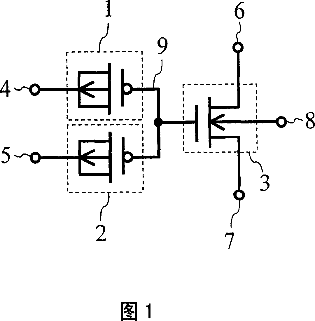
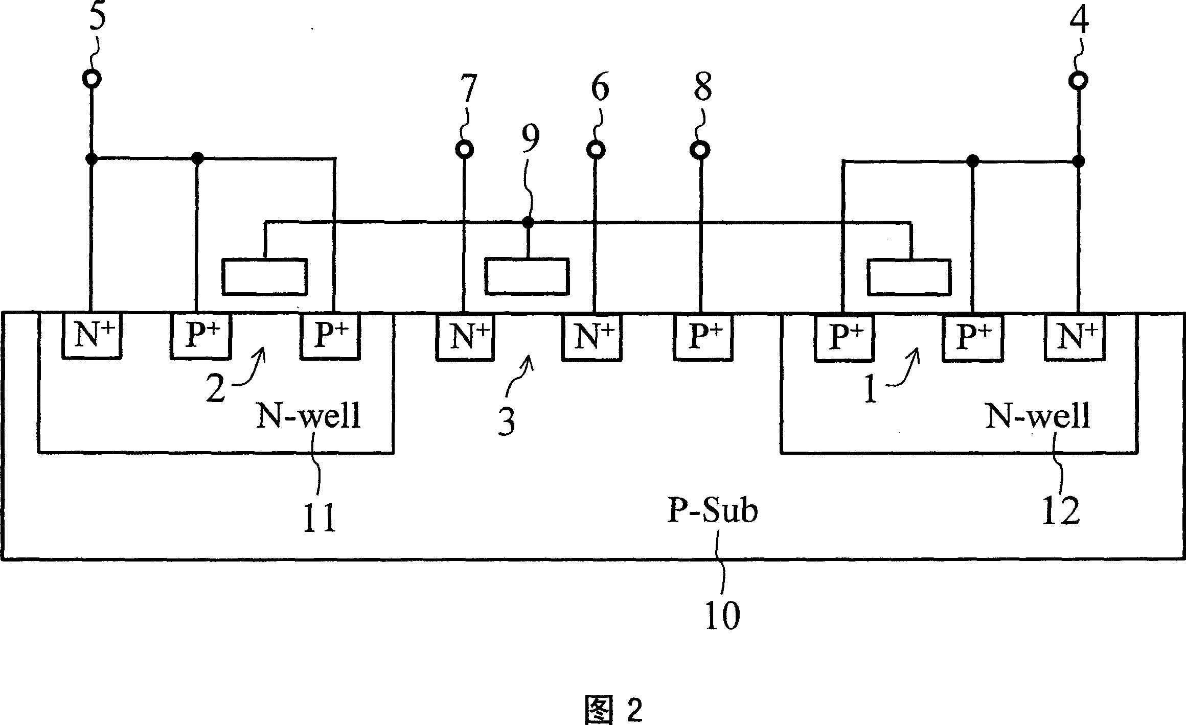
[0068] FIG. 7 shows a circuit diagram of the nonvolatile memory element in the first embodiment of the present invention, and FIG. 8 shows its cross-sectional view. The nonvolatile memory element of the present invention is composed of three transistors in which the control gate transistor 24 is PMOS, the readout transistor 26 is NMOS, and the erasing gate transistor 25 is N-type DMOS. , called "PMOS-NMOS-DMOS (PND) unit".
[0069] In Fig. 7, 27 is the control gate (CG), 28 is the elimination gate (EG), 29 is the drain terminal of the NMOS transistor, 30 is the source terminal of the NMOS transistor, 31 is the P-type silicon substrate terminal, and 32 is the floating Gate (FG). In FIG. 8, 33 and 34 are N-type well regions, and 35 is a P-type silicon substrate. The polysilicon gates of PMOS 24 , NMOS 26 , and N-type DMOS 25 are electrically connected to form floating gate (FG) 32 of the nonvolatile memory element. The N-type well region 34 of the PMOS 24 serves as the contro...
no. 2 Embodiment approach 》
[0074] FIG. 11 is a circuit diagram of a nonvolatile semiconductor memory device configured with differential cells in a second embodiment of the present invention. One of the differential bit units is called a T (True) bit, and the other is called a B (Bar) bit. Here, 45 is a T-bit control gate transistor (PMOS transistor), 46 is a T-bit erasing gate transistor (N-type DMOS transistor), 47 is a T-bit readout transistor (NMOS transistor), and 48 is a load PMOS transistor. Transistor, 49 is the control gate transistor (PMOS transistor) of B bit, 50 is the elimination gate transistor (N-type DMOS transistor) of B bit, 51 is the readout transistor (NMOS transistor), 52 is the load PMOS transistor, 53 is Bit line (BL), 54 is a bit line bar ( / BL), and 55 is a sense amplifier.
[0075] 12 is a circuit diagram showing an operation of writing "1" in the configuration of the differential unit in the second embodiment of the present invention. In the operation of writing "1" in the di...
no. 3 Embodiment approach 》
[0082] FIG. 15 shows a circuit diagram of a nonvolatile memory element in a third embodiment of the present invention. Here, 89 is a program gate transistor (PMOS transistor), 90 is a control gate transistor (PMOS transistor), 91 is an erasing gate transistor (PMOS transistor), 92 is a readout transistor (NMOS transistor), and 93 is a program gate transistor. 94 is the control gate (CG), 95 is the elimination gate (EG), 96 is the drain terminal of the NMOS transistor, 97 is the source terminal of the NMOS transistor, 98 is the P-type silicon substrate terminal, 99 is the floating gate (FG).
[0083] FIG. 16 shows a cross-sectional view of a nonvolatile memory element in a third embodiment of the present invention. Here, 100, 101 and 102 are N-type well regions, and 103 is a P-type silicon substrate. In a 3-transistor type nonvolatile memory element, the nonvolatile memory element is constituted by adding 4 transistors with a program gate as another control gate.
[0084] In...
PUM
| Property | Measurement | Unit |
|---|---|---|
| Thickness | aaaaa | aaaaa |
Abstract
Description
Claims
Application Information