
Semiconductor structure and mfg. method thereof

A manufacturing method, semiconductor technology, applied in semiconductor/solid-state device manufacturing, semiconductor devices, electrical components, etc., can solve problems such as damage to thin films, reduced efficiency of Ti absorbing oxygen atoms, inconvenience, etc.

Inactive Publication Date: 2007-04-18
IND TECH RES INST
View PDF0 Cites 19 Cited by
  • Summary
  • Abstract
  • Description
  • Claims
  • Application Information

AI Technical Summary

Problems solved by technology

[0003] In terms of related prior art, Hyoung Kim et al., in "Journal of Applid PhysicsVol.96 No.6, page 3467-3472 (2004)", and the title of the paper is "Engineering chemicallyabrupt high-k metal oxide / Silicon interfaces using an oxygen -gettering metaloverlayer": In HfO 2 (Hafnium dioxide) grows a layer of Ti (titanium) to absorb oxygen atoms and eliminate the interface layer, but then the removal of Ti:O will damage HfO in the process 2 film
Secondly, in Dazhong, Ti is coated by physical vapor deposition (Physical Vapor Deposition, PVD), but the high-energy particles generated in the process will affect the HfO 2 film damage
In addition, in this paper, Ti and HfO 2 The interface layer has a certain distance, so that the efficiency of Ti to absorb oxygen atoms is reduced
[0004] Therefore, it can be seen from the above that the above-mentioned known semiconductor structure obviously has inconvenience and disadvantages in actual use, and can be improved.

Method used


Image

  • Semiconductor structure and mfg. method thereof
  • Semiconductor structure and mfg. method thereof
  • Semiconductor structure and mfg. method thereof

Examples


Embodiment Construction

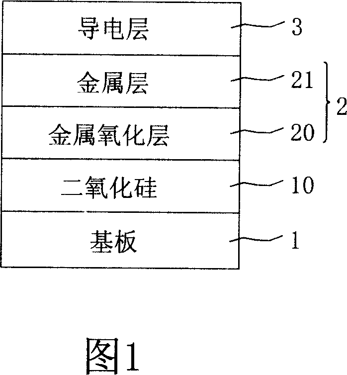
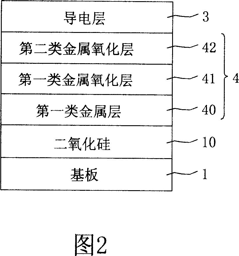
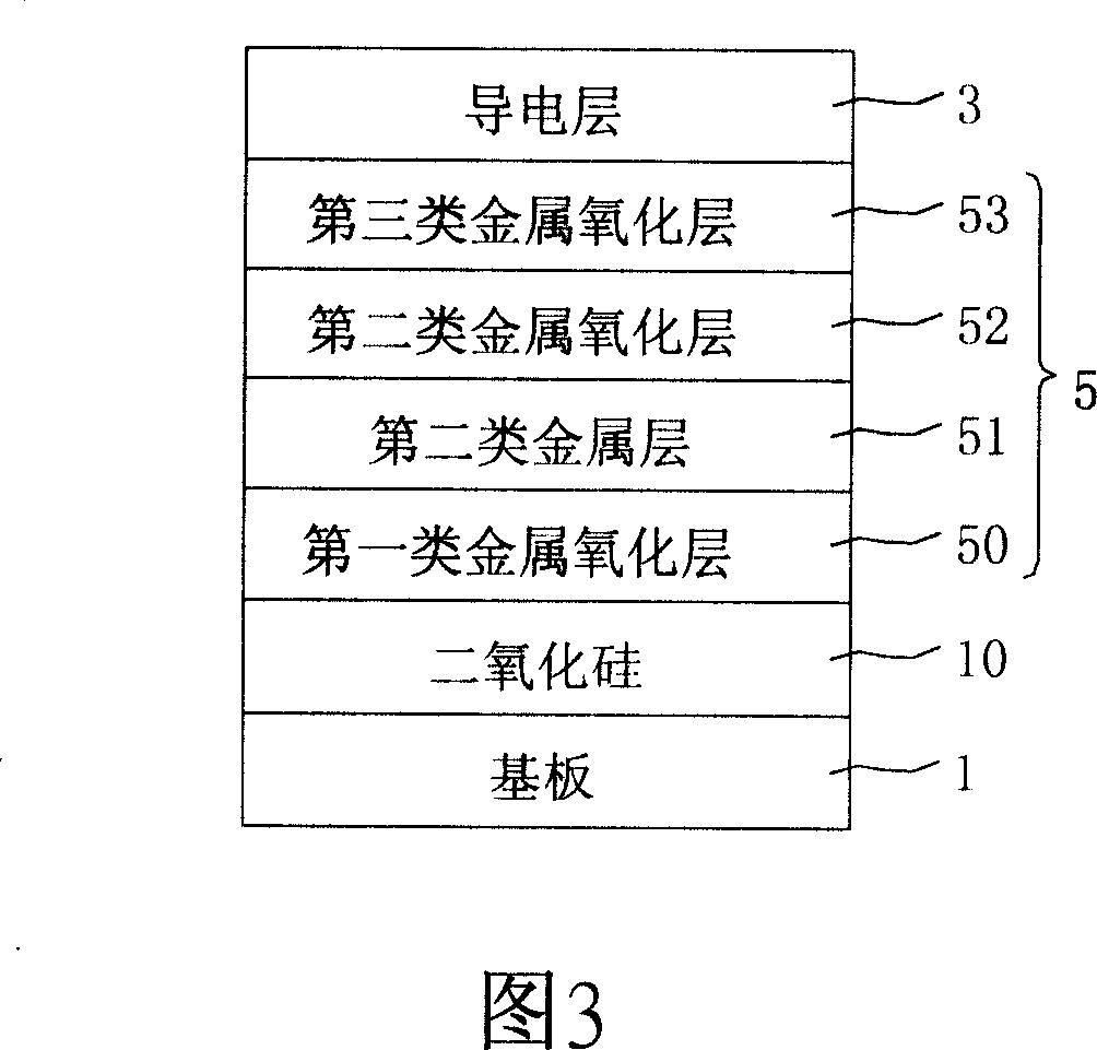
[0041] Please refer to FIG. 1 , which is a schematic cross-sectional view of the first embodiment of the semiconductor structure of the present invention. It can be seen from the figure that the first embodiment of the present invention provides a semiconductor structure, including: a substrate 1 , a dielectric layer unit 2 and a conductive layer 3 .

[0042] Wherein, the substrate 1 can be a silicon substrate (Si substrate), and silicon dioxide 10 (SiO2) is formed on the silicon substrate. 2 ). The dielectric layer unit 2 is formed on the substrate 1, and the dielectric layer unit 2 at least includes a metal oxide layer 20 and a metal layer 21, and the metal oxide layer 20 and the metal layer 21 are formed by stacking each other. The conductive layer 3 is disposed on the dielectric layer unit 2 , and the conductive layer 3 can be titanium nitride (TiN).

[0043] In addition, the metal oxide layer 20 can be hafnium dioxide (HfO 2 ), hafnium oxysilicide (HfSiO), hafnium sili...


PUM

PropertyMeasurementUnit
Thicknessaaaaaaaaaa
Thicknessaaaaaaaaaa

Abstract

The invention relates to a semiconductor structure and the making method, especially relating to an interface layer applied to transistor grid, namely high-dielectric constant semiconductor stacked structure and the making method thereof, using on-HfO2 Ti to absorb oxygen atoms on the interface layer so as to reduce the thickness of the interface layer until no interface layer. And the growth of TiO2 on Ti can help follow-up HfO2 growth. Besides, TiO2 dielectric constant is about 50, able to largely increase equivalent dielectric constant of grid dielectric layer. It can absorb oxygen by Ti to reduce Ti thickness, increase k value and reduce EOT. In addition, after heat treatment, the formed TiO2 can increase k value, too. And in TiO2, leakage current can not leap. And the invention can speed up application of high-dielectric constant grid dielectric and provide a space for future EOT sustained reduction.

Description

technical field [0001] The invention relates to a semiconductor structure and a manufacturing method thereof, in particular to an interface layer applied to a gate of a transistor, that is, a high dielectric constant semiconductor laminated structure and a manufacturing method thereof. Background technique [0002] Usually, in the semiconductor manufacturing method, the function of the so-called dielectric layer (dielectric layer) is used to insulate the electrical signal between the conductive layer and the wire, usually silicon dioxide (SiO2) 2 ), silicon nitride (SiN) and other insulators. In addition, hafnium oxide (HfO) and its silicon nitride (Si x N x ) and other dielectric layers have been considered to be used in transistor gates (gate) in the future, so atomic layer growth technology will be the main technology for depositing this dielectric layer film. However, although the formation of silicon nitride can increase the stability of film formation, it also reduc...

Claims


Application Information

Patent Timeline
IPC IPC(8): H01L29/40H01L29/78H01L21/28H01L21/336
Inventor 裴静伟陈邦旭
Owner IND TECH RES INST
Learn More