Tunnel compensation multiple-active-region infrared detector

An infrared detector and active area technology, applied in semiconductor devices, electrical components, circuits, etc., can solve the problems of high device noise, large device dark current, narrow device absorption spectrum bandwidth, etc., and achieve low power consumption and light response. Fast, low-noise effects

Inactive Publication Date: 2007-04-25
BEIJING UNIV OF TECH
View PDF0 Cites 4 Cited by
  • Summary
  • Abstract
  • Description
  • Claims
  • Application Information

AI Technical Summary

Problems solved by technology

This kind of detector has the following disadvantages: 1. The size of the photocurrent has nothing to do with the number of quantum wells, that is, increasing the number of quantum wells cannot increase the photocurrent; 2. The existence of compensation current is required to ensure stability when the devi

Method used


Image

  • Tunnel compensation multiple-active-region infrared detector
  • Tunnel compensation multiple-active-region infrared detector
  • Tunnel compensation multiple-active-region infrared detector

Examples


Embodiment Construction

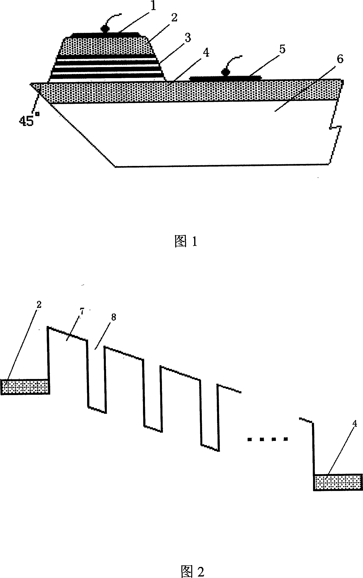
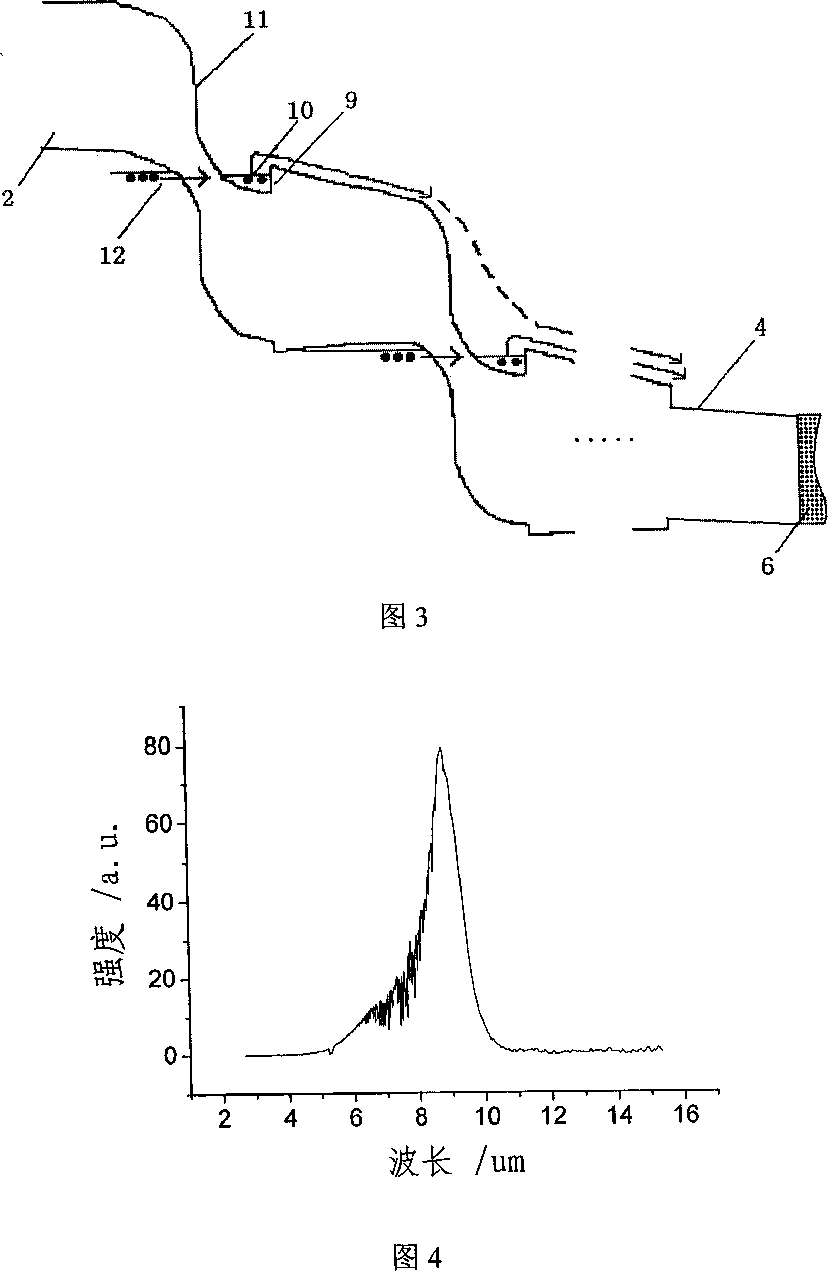
[0038] The device structure of the invention is similar to the traditional multiple quantum well device. Therefore, we can illustrate the device structure of the present invention with the aid of FIG. 1 . The device structure was epitaxially grown by MOCVD. GaAs / Ga 1-x al x As material system as an example: On GaAs semi-insulating substrate 6, epitaxial growth of high-quality n + -GaAs lower contact layer 4, then grow the basic unit (including: p + -Ga 1-x al x As, n + -GaAs and i-Ga 1-x al x As, where by p + -Ga 1-x al x As and n + -GaAs forms a PN junction, i-Ga 1-x al x The As layer forms a potential barrier, the middle n + -GaAs layer forming a potential well) 10 periods. Then grow p + - GaAs upper contact layer 2 . After the structure is grown, the mesa of the device is manufactured according to the GaAs standard photolithography and etching process, and the electrodes 1 and 5 are fabricated on the top and bottom of the mesa. Finally, it is angled, poli...


PUM


Abstract

The invention relates to a tunnel compensate active infrared detector. Wherein, it grows lower contact layer on substrate, grows multi-quantum well, upper contact layer, prepares table and electrode; the invention is characterized in that said multi-quantum well comprises at least one repeat structure formed by at least one basic unit; said basic unit comprises buffer barrier, N-type infrared adsorption area and P-type barrier layer, while they are doped to form tunnel connector; the thickness of buffer barrier is 30-50nm; its forbidden band is wider than the forbidden band of semi-conductor of N-type infrared adsorption area, while bottom of conductor band is higher than the bottom of N-type infrared adsorption area. The invention has high light response, while its light current will increase along the increase of infrared adsorption area, with low hidden current, low power and low noise.

Description

technical field [0001] The invention relates to a medium and long wavelength infrared detection device, in particular to a tunnel compensation multi-active area infrared detector, which belongs to the technical field of semiconductor optoelectronics. Background technique [0002] Traditional medium and long wavelength multiple quantum well or superlattice structure infrared detectors are mainly GaAs / Ga 1-x al x As material system or In x Ga 1-x As / GaAs material system. The realization of its device structure is obtained by molecular beam epitaxy (MBE) or metal organic chemical vapor deposition (MOCVD or OMVPE) technology epitaxial growth. After the standard semiconductor process, the traditional medium and long wavelength multi-quantum well or superlattice structure infrared detection device is obtained, and its basic structure is shown in Figure 1 and 2 (in the form of GaAs / Ga 1-x al x As material system as an example): upper metal electrode 1; upper N-type GaAs conta...

Claims


Application Information

Patent Timeline
IPC IPC(8): H01L31/111
Inventor 沈光地邓军徐晨
Owner BEIJING UNIV OF TECH
Why Eureka
Try Eureka