

Near infrared organic electroluminescent materials and devices and method for fabricating the device
A technology of electroluminescent materials and electroluminescent devices, which is applied in the direction of luminescent materials, electroluminescent light sources, chemical instruments and methods, etc., can solve the problems that the performance of infrared organic light-emitting devices does not meet the application requirements, and achieve easy processing and improved The effect of luminous intensity and simple preparation process
- Summary
- Abstract
- Description
- Claims
- Application Information
AI Technical Summary
Problems solved by technology
Method used
Image

Examples
Embodiment 1
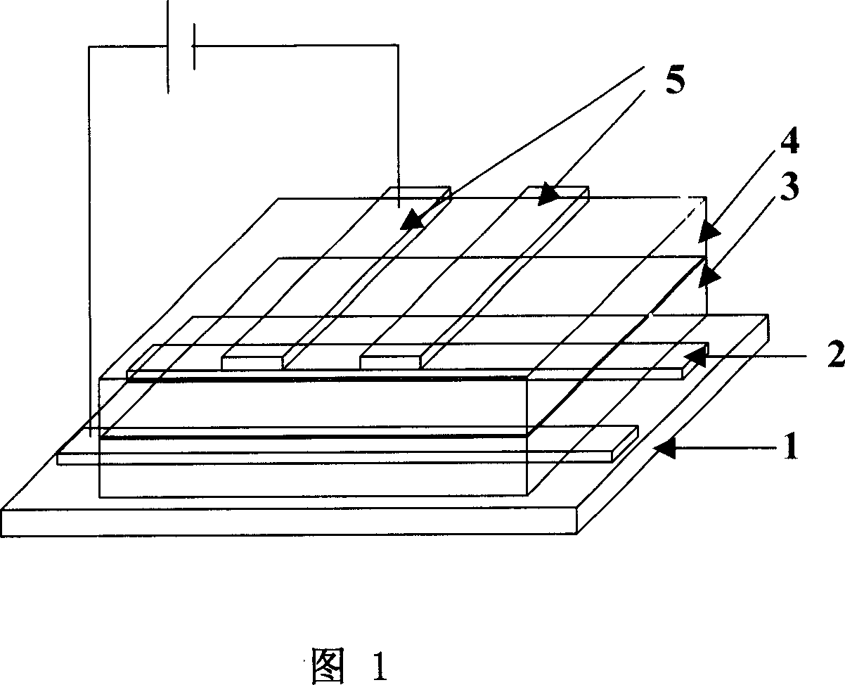
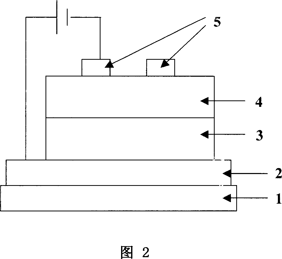
[0035] First, the ITO on the ITO glass is photoetched into electrodes with a width of 5 mm and a length of 30 mm, then cleaned, dried with nitrogen, treated with oxygen plasma for 2 minutes, and immediately spin-coated a layer of PEDOT:PSS conductive polymer on it , put it in an oven and dry at 110°C for 30 minutes to remove moisture, and the thickness of the PEDOT:PSS film is about 50 nanometers. A chloroform solution of infrared dye ADS830AT doped with polyvinyl carbazole (PVK) and cadmium selenide / cadmium sulfide (CdSe / CdS) nanoparticles was spin-coated on PEDOT:PSS to obtain a luminescent layer with a thickness of 100 nm. Then transfer it to the vacuum coating system until the vacuum degree reaches 1-5×10 -1 Pascal deposited 200nm-thick metal Al on the light-emitting layer to prepare an infrared organic electroluminescent device with a structure of ITO / / PEDOT:PSS / / ADS830AT:CdSe / CdS:PVK / / Al. Wherein the evaporation rate of the Al electrode is controlled at 5 nanometers per...
Embodiment 2
[0037] First, the ITO on the ITO glass is photoetched into electrodes with a width of 5 mm and a length of 30 mm, then cleaned, dried with nitrogen, treated with oxygen plasma for 2 minutes, and immediately spin-coated a layer of PEDOT:PSS conductive polymer on it , put it in an oven and dry at 110°C for 30 minutes to remove moisture, and the thickness of the PEDOT:PSS film is about 50 nanometers. A chloroform solution of polyvinylcarbazole (PVK) blended with infrared dye ADS830AT doped with cadmium telluride (CdTe) nanoparticles was spin-coated on PEDOT:PSS to obtain a luminescent layer with a thickness of 100 nanometers. Then transfer it to the vacuum coating system until the vacuum degree reaches 1-5×10 -4 At Pascal, 200nm-thick metal Al was vapor-deposited on the light-emitting layer to prepare an infrared organic electroluminescent device with a structure of ITO / / PEDOT:PSS / / ADS830AT:PVK-CdTe / / Al, wherein the evaporation rate of the Al electrode Controlled at 5 nanometers...
Embodiment 3
[0039] First, the ITO on the ITO glass is photoetched into electrodes with a width of 5 mm and a length of 30 mm, then cleaned, dried with nitrogen, treated with oxygen plasma for 2 minutes, and immediately spin-coated a layer of PEDOT:PSS conductive polymer on it , placed in an oven and dried at 110°C for 30 minutes to remove moisture, and the thickness of the PEDOT:PSS film was about 50 nanometers. A chloroform solution of infrared dye ADS830AT doped with polyvinyl carbazole (PVK) and cadmium selenide / cadmium sulfide (CdSe / CdS) nanoparticles was spin-coated on PEDOT:PSS to obtain a luminescent layer with a thickness of 100 nm. Then transfer it to the vacuum coating system, wait until the vacuum degree reaches 1-5×10 -4 At Pascal, 200nm-thick metal Al was vapor-deposited on the light-emitting layer to prepare an infrared light with a structure of ITO / / PEDOT:PSS / / ADS830AT:CdSe / CdS:PVK (1:9:40, weight ratio) / / Al Organic electroluminescent devices. Wherein the evaporation rate...
PUM
| Property | Measurement | Unit |
|---|---|---|
| thickness | aaaaa | aaaaa |
| wavelength | aaaaa | aaaaa |
| thickness | aaaaa | aaaaa |
Abstract
Description
Claims
Application Information