Lead frame for integrated circuit or discrete components ultra-thin non-pin packing

A technology of discrete components and integrated circuits, applied in the direction of electrical components, circuits, electrical solid devices, etc., can solve the problems of high electroplating cost, discounted flexibility, slow heat dissipation rate, etc., and achieve low material cost, stable quality, and high efficiency. Effect

Active Publication Date: 2007-07-04
长电科技管理有限公司
View PDF0 Cites 1 Cited by
  • Summary
  • Abstract
  • Description
  • Claims
  • Application Information

AI Technical Summary

Problems solved by technology

[0004] 2. In order to make the wire bonding process and output solder joints can be produced smoothly in this process, expensive palladium materials are plated on both sides of the substrate. In addition to the relatively high cost of electroplating, the wire bonding parameters should also be set for this material Special parameters, which directly affect the smoothness of the production line due to the inconsistency of the parameters
[0005] 3. The substrate is usually made of CU194, which has a conductivity of only A5% and a relatively slow heat dissipation rate. It is only suitable for general logic or low-power products.
[0006] 4. Because of the use of special chemical tape and the solvent of the tape in various high-temperature processes is easy to vaporize due to high temperature, the aluminum pad that indirectly pollutes or covers the chip, that is, the inner foot of the wire, often causes the instability of the wire bonding ability
[0007] 5. Because this product is made of plastic and copper, the same blade and blade rotation speed cannot be used to divide the array integrated circuit or discrete component assembly under different materials, and the two blades cannot be the same, and if When forcing the use of the same blade, that is, the speed parameter, the life of the blade will be greatly reduced. Of course, the maintenance cost and quality will be affected to a certain extent.
[0008] 6. Due to the limitation of traditional technology, solder joints with multiple chips and different outputs can only be arranged in a rigid manner, and the flexibility is greatly reduced.
[0009] 7. Due to the limitations of the traditional process, the output solder joints are as flat as the bottom of the plastic package, and there is even a risk of dents. However, it is impossible to mount flux, rust remover and other chemicals on the surface. It is discharged smoothly, so it will be greatly reduced in terms of solderability

Method used


Image

  • Lead frame for integrated circuit or discrete components ultra-thin non-pin packing
  • Lead frame for integrated circuit or discrete components ultra-thin non-pin packing
  • Lead frame for integrated circuit or discrete components ultra-thin non-pin packing

Examples


Embodiment Construction

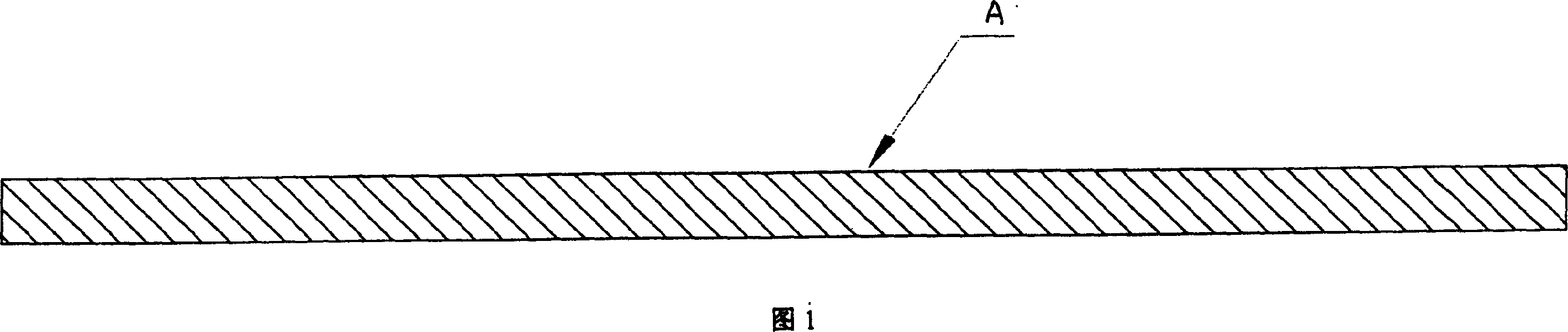
[0026] 1) Referring to Figure 1, take a piece of metal substrate A with a suitable thickness. The material of the metal substrate can be changed according to the function and characteristics of the chip, such as: alloy or copper;

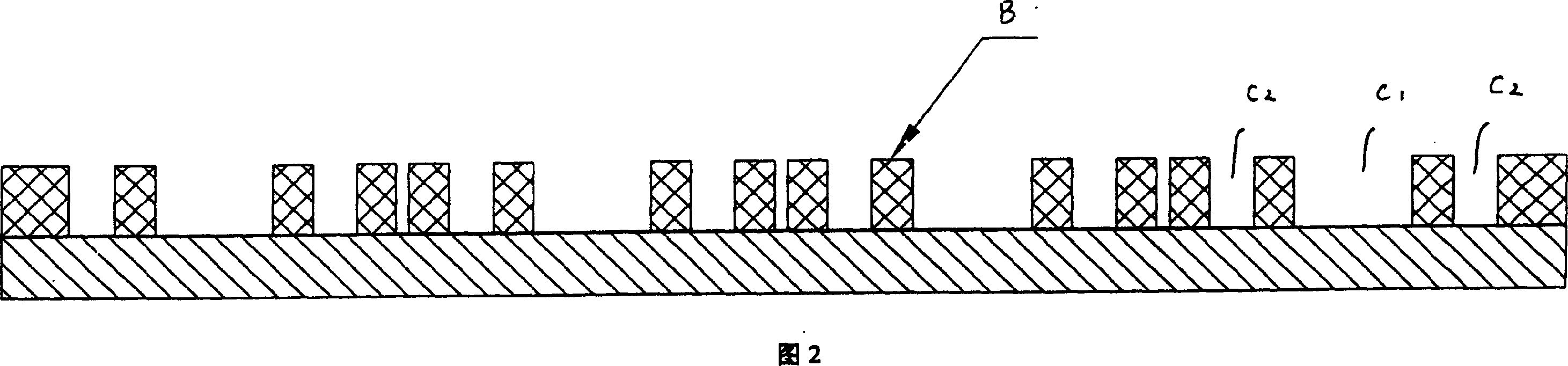
[0027] 2) Referring to FIG. 2, dry ink B coating is carried out on the metal substrate A. The area on the metal substrate that is not coated with dry ink forms the chip area C1 and the inner foot area C2 for wiring;

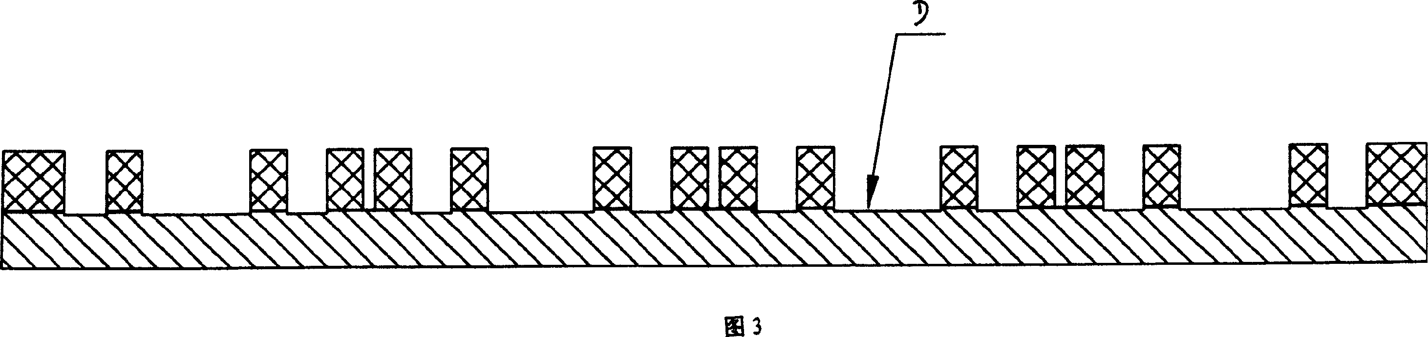
[0028] 3) Referring to FIG. 3, etch the chip area C1 and the inner foot area C2 of the wiring on the metal substrate;

[0029] 4) Referring to FIG. 4, a layer of pure metal layer 1 is sputtered on the metal substrates A1 and A2 in the chip area C1 and the wire bonding inner pin area C2;

[0030] 5) Referring to FIG. 5, on the pure metals 11 and 12 in the chip area C1 and the wire-bonding inner foot area C2, a layer of metal activation layer 2 is sputtered, such as an aluminum layer or a nickel, titanium, silver, or gold layer;

[00...


PUM


Abstract

This invention relates to an IC or discrete component super-thin leg-free packaging leading-line frame, including the substrate, the chip bearing base and the fight line inward-feet bearing base, the chip bearing base and the fight line inward-feet bearing base protruding upward to set up on the substrate surface, and corresponding to the chip bearing base and the fight line inward-feet bearing base, the substrate has corresponding chip region and the fight line inward-feet to depress on the substrate surface; the chip bearing base and the fight line inward-feet base bottom being the metal layer (11,12); above the chip bearing base and the fight line inward-feet base metal layer, first sputtering a metal activation layer (2), and then sputtering a copper metal or alloy layer (31, 32); above the fight line inward-feet bearing base copper metal or alloy layer, sputtering a silver metal, or nickel metal, or palladium metal layer (52). This invention has strong welding performance, excellent quality, lower costs, smoother production, and strong applicability, and for cutting tools and blades, it can play a maximum efficiency, multi-chip arranged flexibly, no plastic infiltration or other various difficulties, and for the environment protection.

Description

Technical field: [0001] The invention relates to an integrated circuit or discrete component ultra-thin non-pin packaging process and its packaging structure, in particular to a lead frame for integrated circuit or discrete component ultra-thin non-pin package. It belongs to the technical field of packaging of integrated circuits or discrete components. Background technique: [0002] The traditional ultra-thin and footless packaging process of integrated circuits or discrete components and its packaging structure, its packaging type is an array-type assembly that is cut into a single unit. Its substrate type is etched. It mainly has the following deficiencies: [0003] 1. Special adhesive tape is required. In order to prevent the plastic from penetrating into the lead frame during high-pressure encapsulation, increasing the risk of solder joint insulation, and if the post-treatment of plastic penetration occurs, it is easy to destroy the metal layer of the solder joint. A...

Claims


Application Information

Patent Timeline
Patent Type & Authority Applications(China)
IPC IPC(8): H01L23/495
CPCH01L2924/0002
Inventor 梁志忠黄能捷韩蔚华
Owner 长电科技管理有限公司
Why Eureka
Try Eureka