Circuit board, method for manufacturing the same, semiconductor device, and method for manufacturing the same

A technology for circuit substrates and manufacturing methods, which is applied in semiconductor/solid-state device manufacturing, semiconductor devices, semiconductor/solid-state device components, etc., and can solve the problem of reduced semiconductor device yield and connection reliability, and the reduction of the gap between semiconductor chips and circuit substrates , reduced joint height, etc., to achieve high yield, easy contact, and increased clearance

Inactive Publication Date: 2007-07-11
PANASONIC CORP
View PDF1 Cites 7 Cited by
  • Summary
  • Abstract
  • Description
  • Claims
  • Application Information

AI Technical Summary

Problems solved by technology

However, if the bump size is small, the amount of gap between the semiconductor chip and the circuit board will be small because the junction height is reduced
Therefore, the fillability of the filler deteriorates, and there is a problem that the yield and connection reliability of semiconductor devices are lowered.

Method used


Image

  • Circuit board, method for manufacturing the same, semiconductor device, and method for manufacturing the same
  • Circuit board, method for manufacturing the same, semiconductor device, and method for manufacturing the same
  • Circuit board, method for manufacturing the same, semiconductor device, and method for manufacturing the same

Examples


Embodiment 1

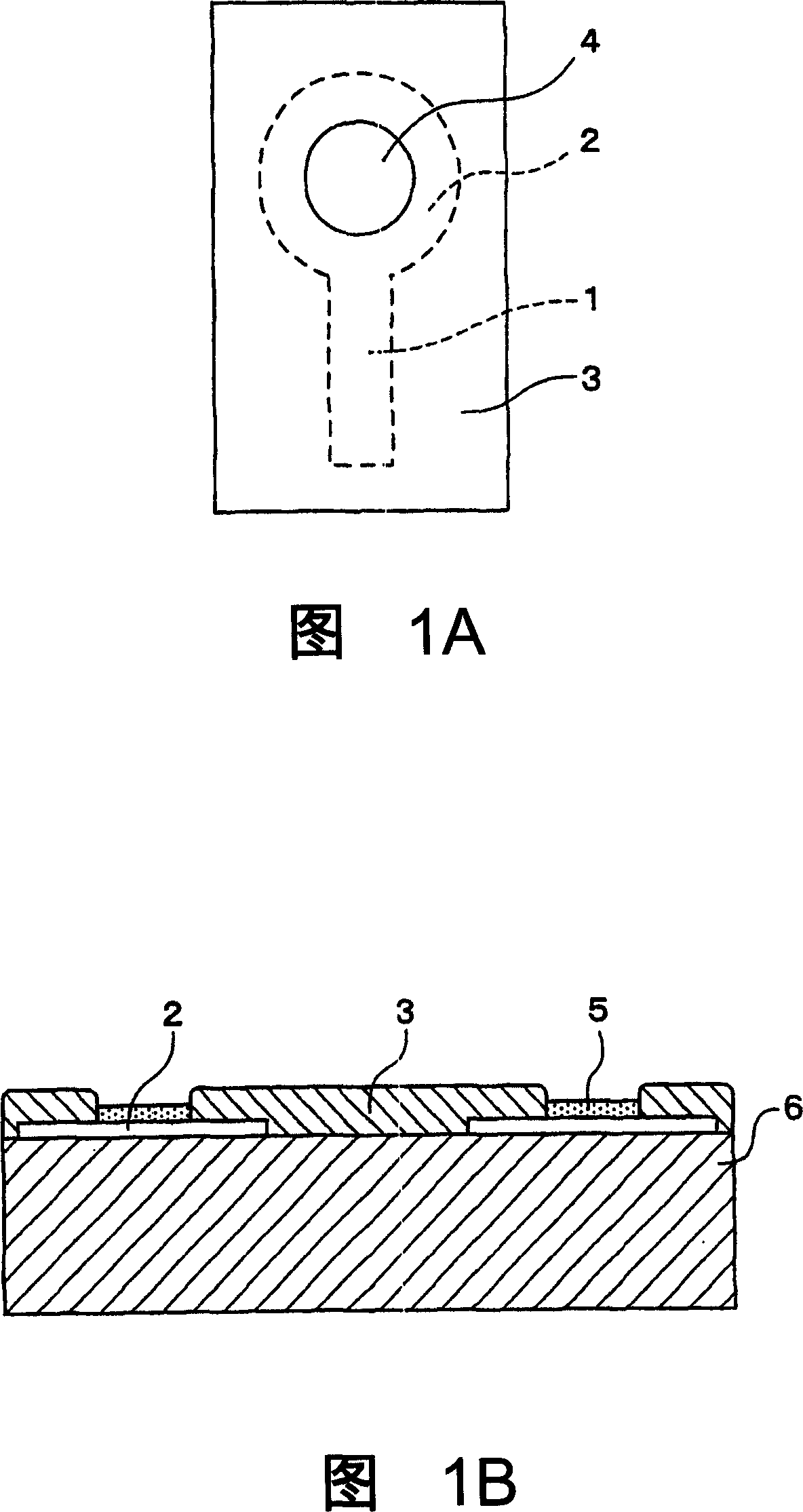
[0114] In Example 1, as the TEG (Test Element Group) for evaluation, a chip having a size of 10 mm x 10 mm, a thickness of 300 μm, electrodes formed with 900 pins, and a segmented array formed at 250 μm intervals was used. On the electrodes (pads) of the TEG for evaluation, Sn—Ag solder bumps with a radius of 55 μm were formed.

[0115] On the other hand, a general glass epoxy double-sided copper-clad board (manufactured by Hitachi Chemical Co., Ltd.: product name [MCL-E-67], thickness 1.6 mm) was prepared as a circuit board, and on the surface layer of the double-sided copper-clad board, use The pattern of wiring (wiring patterns and pattern wiring) and connection pads (main electrodes) is formed with a pitch of 250 μm and a diameter of 200 μm by photolithography. Here, in order to be able to evaluate bonding properties when semiconductors are mounted, the patterns of wiring and connection pads are configured so that electrodes on the TEG side for evaluation and electrodes on...

Embodiment 2

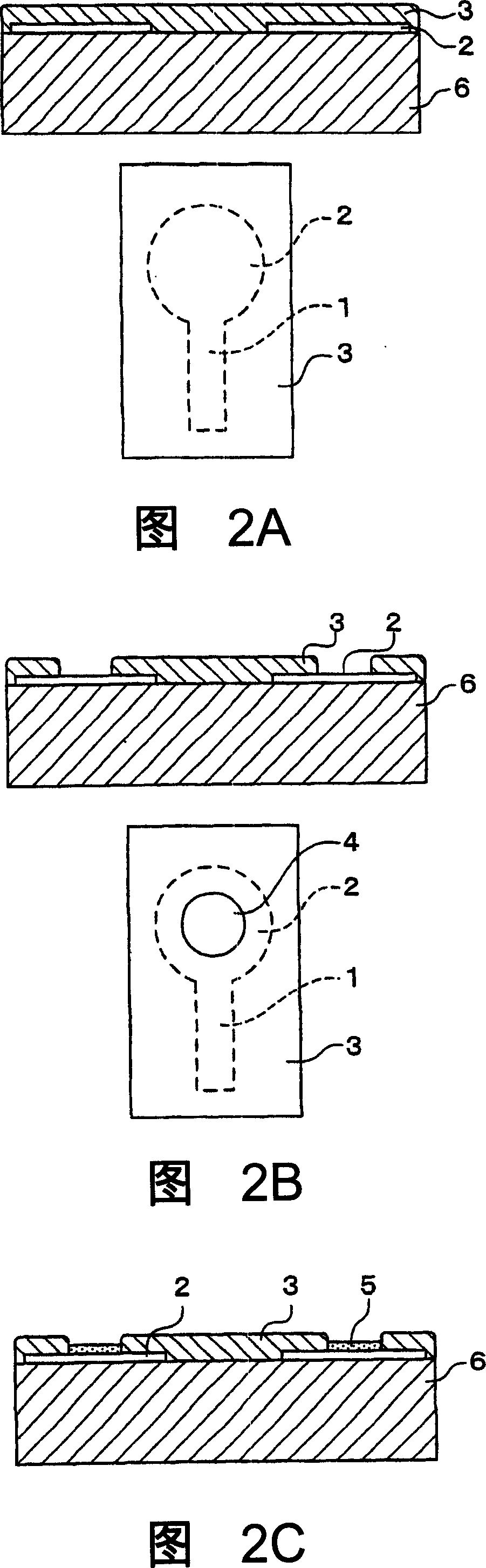
[0130] In this embodiment 2, as the semiconductor chip, the same chip as that in embodiment 1 is used. The same circuit board and solder resist as in Example 1 were also used. In addition, the same four conditions as in Example 1 of 40, 60, 80, and 100 μmφ were used for the diameter of the solder resist opening.

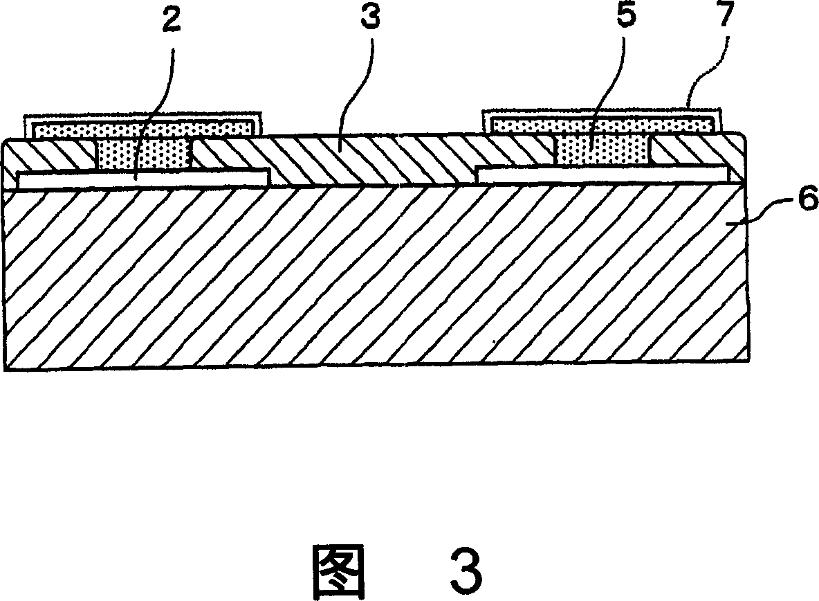
[0131] In Example 2, after the solder resist opening was formed, a printing mask having an opening with a diameter of 200 μmφ larger than the opening was placed on the solder resist, and the silver paste was filled by printing through the screen mask ( Manufactured by Vacuum Metallurgical Co., Ltd. (currently Albac Material Co., Ltd.: product name [nanope st]), and fired at 230° C. for 1 hour to produce a circuit board for flip-chip mounting. Next, a semiconductor chip (TEG for evaluation) was mounted in the same manner as in Example 1, and a flip-chip semiconductor device was obtained through a solvent cleaning step and a filler injection step.

[0132] As in Exam...


PUM


Abstract

A circuit board for flip-chip packaging is provided which can achieve the connection reliability of a semiconductor device and the circuit board. The circuit board for flip-chip packaging includes, on a surface of a substrate ( 6 ), wiring patterns ( 1 ), connection pads ( 2 ) for flip-chip packaging, and a solder resist ( 3 ) having openings ( 4 ) formed on the connection pads ( 2 ). In the circuit board, conductive members ( 5 ) are formed in the openings ( 4 ).

Description

technical field [0001] The present invention relates to a circuit substrate for solder-joint flip-chip mounting and a manufacturing method thereof, and a semiconductor device for mounting a semiconductor chip by a flip-chip mounting process and a manufacturing method thereof. Background technique [0002] In recent years, as electronic devices such as portable information devices have become smaller, thinner, and lighter, semiconductor devices (semiconductor modules) have been required to have higher densities and higher performance. In addition, along with the increase in performance of semiconductor chips, there is a remarkable tendency to increase the number of pins in semiconductor chips. In addition, at the same time, the operating frequency of semiconductor chips is also becoming higher and higher. In order to meet these demands, a semiconductor device in which a semiconductor chip is mounted by a flip chip mounting process has been developed. [0003] The flip-chip ...

Claims


Application Information

Patent Timeline
Patent Type & Authority Applications(China)
IPC IPC(8): H01L23/498H01L21/48H05K1/02H05K3/00
CPCH05K2201/035H01L24/10H01L2924/01046H05K2201/099H01L2924/0105H01L2924/01082H05K3/244H01L2224/8191H01L2924/01049H01L2224/81801H05K1/113H01L2924/01019H01L2924/01029H05K2201/09436H01L2224/13099H01L23/49822H01L2924/01027H05K2201/10674H01L2924/014H01L23/49838H01L2924/01013H01L2924/0103H05K3/3452H01L24/81H01L2924/01047H05K2201/0191H05K3/245H01L2924/01079H01L23/498H01L2224/81815H01L2224/81136H01L23/49811H01L2924/01005H01L2924/01033H01L2924/01006H01L2924/01074H01L2924/01078H01L2224/8121H05K3/3436H01L2924/01051H01L24/13H01L2224/10175H01L2224/13Y02P70/50H01L2924/00
Inventor 藤井俊夫
Owner PANASONIC CORP
Why Eureka
Try Eureka