Supercharge Your Innovation With Domain-Expert AI Agents!

Method for obtaining a bonding surface for direct bonding

a technology of direct bonding and bonding surface, which is applied in the direction of transportation and packaging, basic electric elements, solid-state devices, etc., can solve the problems of high cost, inability to use in numerous applications that involve components based on semiconductor materials, and material gain at the expense of sintered substrate quality, so as to reduce the prime cost

Active Publication Date: 2018-07-24
COMMISSARIAT A LENERGIE ATOMIQUE ET AUX ENERGIES ALTERNATIVES
View PDF3 Cites 0 Cited by
  • Summary
  • Abstract
  • Description
  • Claims
  • Application Information

AI Technical Summary

Benefits of technology

This patent is about a method that allows for a strong bond between metallic and flexible substrates without the need for adhesive or solder. The method involves a combination of steps that results in a smooth surface that can be easily bonded. The resulting structure is durable and can withstand temperature changes. The materials used are inexpensive, making it suitable for a variety of applications, including consumer products. Overall, this method offers a cost-effective way to create strong and durable bonds between metallic and flexible substrates.

Problems solved by technology

However, their high cost makes their use impossible in numerous applications that involve components based on semiconductor materials.
However, the gain in the cost of the material is done at the expense of the quality of the sintered substrates.
Consequently, the sintered substrates are much more difficult to prepare, and in particular to polish, than the electro-fused material substrates whose behavior is much more predictable.
In order to prepare these sintered substrates, different methods exist but they do not allow to obtain a satisfactory surface condition for a direct metallic bonding (RMS roughness<1 nm, absence of scratches, good flatness, etc.) within the conventional processes windows.
For example, the mechanical polishing allows to obtain good surface conditions in terms of RMS roughness but it introduces numerous defects where scratch is the main expression.
Moreover, the mechano-chemical polishing does not allow obtaining a satisfactory surface condition.
Even though at the grain scale, a good roughness is obtained (RMS roughness<1 nm), the action of the chemical reactant remains highly sensitive to the nature and orientation of the grains and it is highly difficult to find stable conditions that can enable smoothing and planarization of the surface at the same time.
Nonetheless, a copper layer is introduced in the structure and due to the differences in CTE between the materials (Si / / Cu / / Mo), this layer causes reliability problems and failure modes by fatigue of the structure.
Thus, if step a) is directly followed by steps c) and d) or only by step d), a revelation of the grains is observed at the surface leading to a surface condition that is incompatible with the direct bonding technique.
Moreover, if steps b) to d) are carried out on a surface condition that is different from that of the base substrate of step a), the surface roughness that is compatible with a direct bonding is harder to obtain.
Thus, the defects that are created at the base surface by the ion bombarding of step b) are not restored by this thermal energy supply in the metallic layer.

Method used


Image

  • Method for obtaining a bonding surface for direct bonding
  • Method for obtaining a bonding surface for direct bonding

Examples


Embodiment Construction

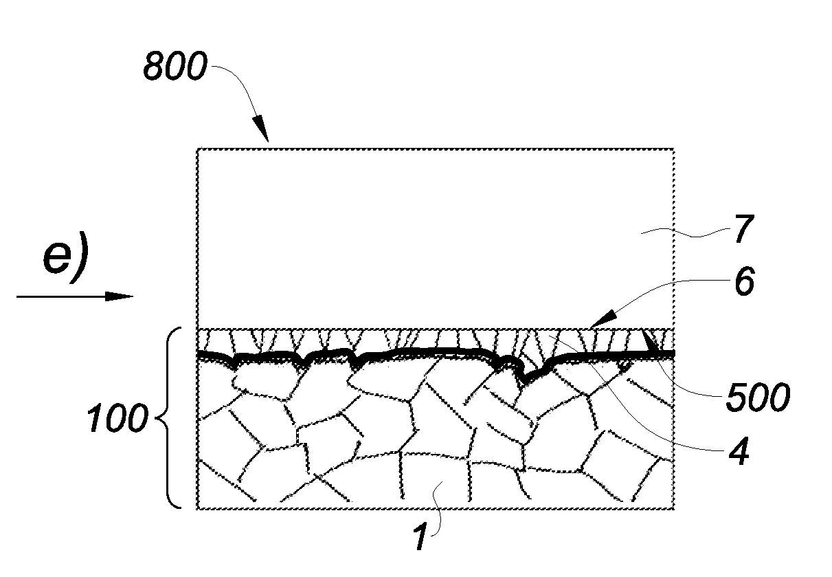
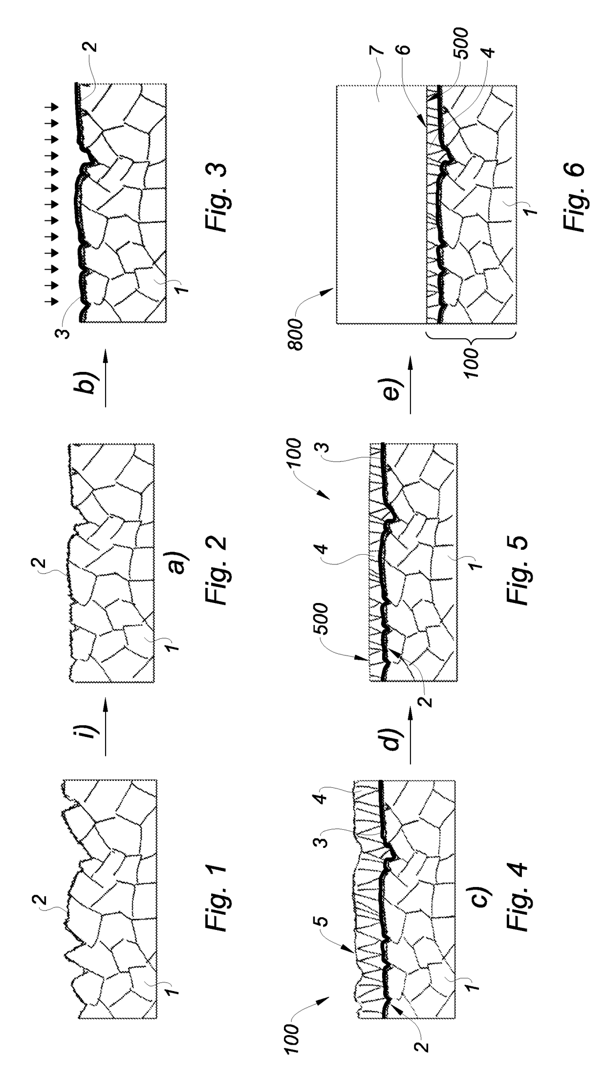
[0054]FIG. 1 illustrates a solid metallic base substrate 1 made of sintered molybdenum, whose base surface 2 presents a RMS roughness comprised between 20 and 30 nanometers over a 5*5 μm2 field and a PV roughness comprised between 150 and 250 nanometers measured by optical interferometry over a 100*100 μm2 field. These characteristics correspond to the typical characteristics of sintered substrates that are currently in the market.

[0055]More generally, the base substrate 1 may be formed of a sintered refractory metal such as molybdenum, tungsten, tantalum, rhenium or niobium and an alloy of these metals.

[0056]FIG. 2 illustrates the step i) of the method which consists in performing a mechanical polishing on the base surface 2, for example with an aqueous solution of diamond on an abrasive pad. The RMS roughness of the base surface 2 obtained after this polishing is comprised between 2 and 6 nanometers, the PV roughness of the base surface 2 is comprised between 25 and 100 nanometers...


PUM

PropertyMeasurementUnit
PV roughnessaaaaaaaaaa

Abstract

A process for obtaining a bonding surface for direct bonding includes: a) providing a substrate based on a sintered metal having a base surface with an RMS roughness lower than 6 nanometers and a PV roughness lower than 100 nanometers; b) bombarding the base surface with ionic species; c) depositing a metal layer on the base surface; and d) carrying out a mechanical and / or chemical polish of an exposed surface of the metal layer. A structure including a substrate based on a sintered metal the base surface of which is at least partially formed from a metal including ionic species implanted by bombardment of the base surface, and a metal layer of identical chemical composition to that of the metal base substrate and including a bonding surface with an RMS roughness lower than 0.6 nanometers and a PV roughness lower than 10 nanometers is also provided.

Description

BACKGROUNDTechnical Field[0001]The present invention concerns a method for obtaining a bonding surface of a sintered metallic support substrate in order to perform a direct bonding on a receiver substrate. The invention also concerns a structure comprising a sintered metallic support substrate bonded by direct bonding to a receiver substrate comprising a functionalized layer of a semiconductor material.Related Art[0002]In the semiconductor materials industry, direct metallic bonding is a widely used technology for ensuring assembly of two substrates presenting metallic bonding layers, and in particular, for leading to functionalized 3D structures.[0003]Nowadays, in an increasing number of applications such as lighting, photovoltaics and power, it turns out to be interesting to use direct bonding for assembling substrates that are functionalized by components for LEDs, solar cells, power diodes or transistors, etc. with solid metallic substrates. Not only direct bonding is reliable b...

Claims


Application Information

Patent Timeline
Patent Type & Authority Patents(United States)
IPC IPC(8): H01L23/00H01L21/18H01L33/00
CPCH01L24/83H01L21/187H01L33/0079H01L2224/83031Y10T428/12528H01L2924/12041H01L2924/12043H01L2924/157Y10T428/12493H01L2224/83047H01L33/0093
Inventor BENAISSA, LAMINEGONDCHARTON, PAULIMBERT, BRUNO
Owner COMMISSARIAT A LENERGIE ATOMIQUE ET AUX ENERGIES ALTERNATIVES
Features
  • R&D
  • Intellectual Property
  • Life Sciences
  • Materials
  • Tech Scout
  • Unparalleled Data Quality
  • Higher Quality Content
  • 60% Fewer Hallucinations
Learn More