Electronic circuit package using composite magnetic sealing material

a technology of composite magnetic sealing and electronic circuits, applied in magnetic materials, basic electric elements, magnetic bodies, etc., can solve problems such as conventional composite magnetic sealing materials, and difficult to solve malfunction and radio disturbance, and achieve enhanced electromagnetic shielding characteristics, higher conductivity, and high permeability

Active Publication Date: 2019-09-03
TDK CORPARATION
View PDF25 Cites 4 Cited by
  • Summary
  • Abstract
  • Description
  • Claims
  • Application Information

AI Technical Summary

Benefits of technology

[0017]According to the present invention, by using the first filler having a low thermal expansion coefficient, it is possible to significantly reduce the thermal expansion coefficient of the molding member formed of a composite magnetic sealing material to, e.g., 15 ppm / ° C. or less. This can prevent warpage of the substrate, interfacial peeling in the molding material, cracking of the molding material, and the like. Further, the molding member has both conductivity and magnetism, so that it is possible to obtain a composite shielding structure having both an electromagnetic shielding function and a magnetic shielding function by the molding member itself.
[0028]In the present invention, the thickness of the composite molding member at a portion above the electronic component may be equal to or larger than 50 μm, or equal to or larger than 100 μm and equal to or smaller than 300 μm. With this configuration, it is possible to obtain higher shielding characteristics than in a case where the surface of a general molding member is shielded by a metal film as well as to achieve reduction in height.

Problems solved by technology

However, this tendency poses a problem of malfunction and radio disturbance due to noise.
The problem of malfunction and radio disturbance is difficult to be solved by conventional noise countermeasure techniques.
However, conventional composite magnetic sealing materials have a drawback in that it has a large thermal expansion coefficient.
Thus, a mismatch occurs between a composite magnetic sealing material and a package substrate or electronic components in terms of the thermal expansion coefficient.
As a result, an aggregated substrate having a strip shape after molding may be greatly warped, or there may occur a warp large enough to cause a problem with connectivity of an electronic circuit package in a diced state in mounting reflow.
On the other hand, the difference in physical properties between semiconductor ICs and electronic components mounted on a substrate and a molding material also generates a stress, causing various problems such as interfacial delamination of the molding material and crack of the electronic components or molding material.
H10-64714, the composite magnetic sealing material obtained by adding general soft magnetic powder to a mold resin cannot achieve a target small thermal expansion coefficient.
S59-132196, the covering of the entire structure with the metal casing makes reduction in height difficult.
Further, the metal casing has a large number of holes formed therein and is not connected to a ground pattern of a substrate, so that a sufficient shielding effect cannot be obtained.

Method used


Image

  • Electronic circuit package using composite magnetic sealing material
  • Electronic circuit package using composite magnetic sealing material
  • Electronic circuit package using composite magnetic sealing material

Examples


examples

[0108]First filler F1 having a median diameter (D50) of 10 μm and second filler F2c having a median diameter (D50) of 0.7 μm were prepared. The first filler F1 was formed of an Invar material with 64 wt. % of Fe and 36 wt. % of Ni, and an Ag having 50 nm thickness was plated on the surface thereof. The second filler F2c was formed of a heat resistant resin, and Ag having a thickness of 80 nm was plated on the surface thereof.

[0109]Then, a biphenyl type epoxy resin, a phenol novolac type curing agent, and a catalyst (imidazole) were dissolved in butyl carbitol to prepare a binder. The above first filler F1 and second filler F2c were put into the binder, followed by stirring and kneading in a kneader, to obtain a pasty composite sealing material. The blending ratios of the first filler F1, second filler F2c, and binder in the composite sealing material were 50 vol. %, 25 vol. %, and 25 vol. %, respectively.

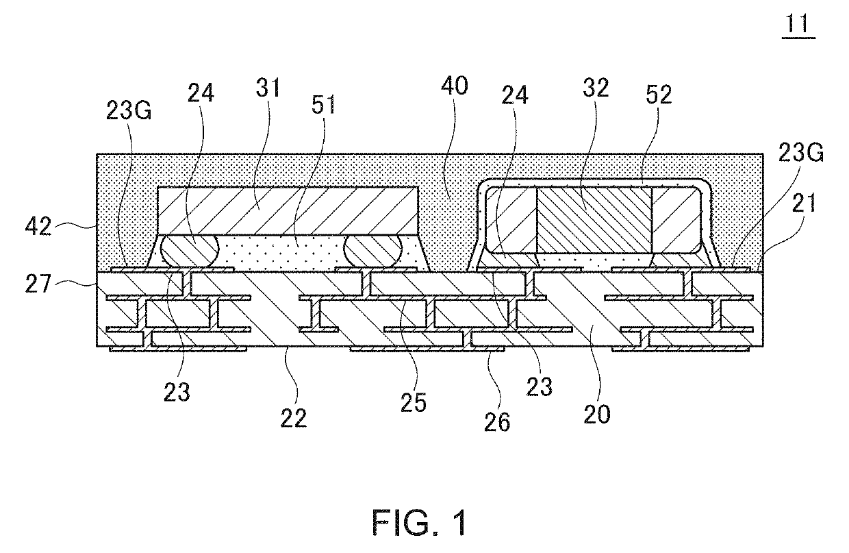
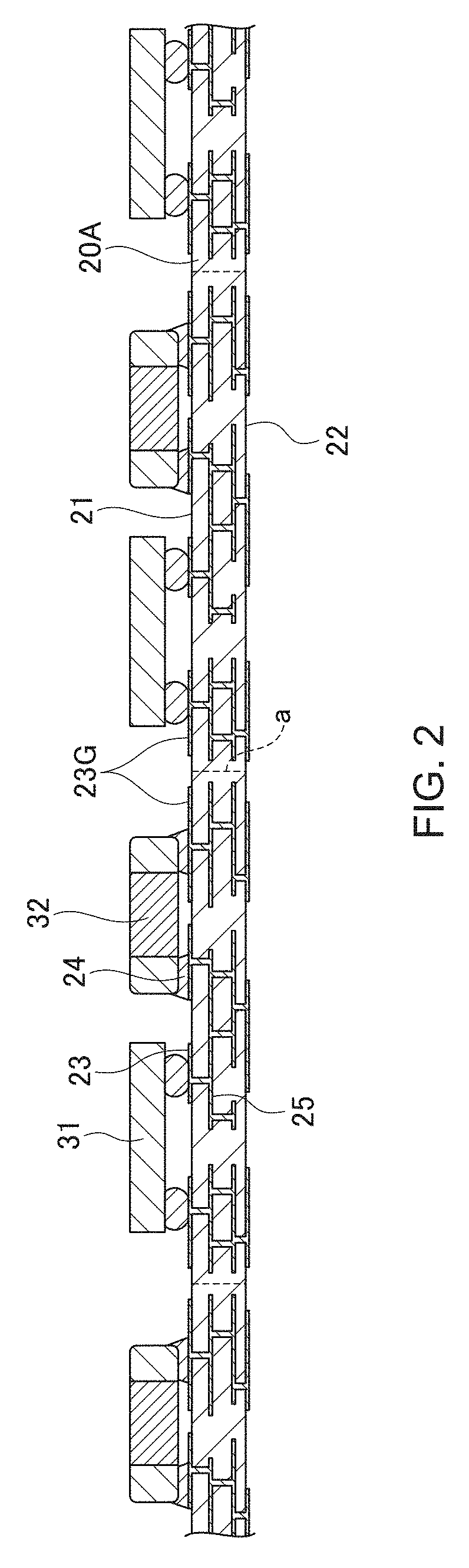
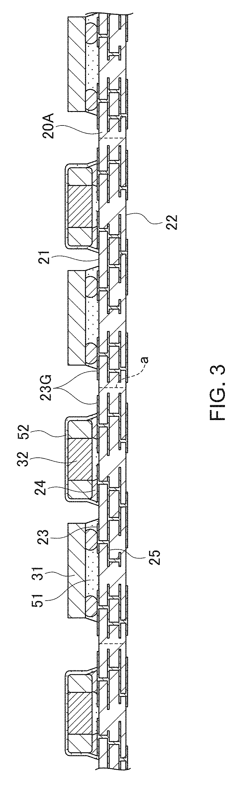
[0110]Then, samples 1 to 3 having the same structure as that of the electronic ...


PUM

PropertyMeasurementUnit
thicknessaaaaaaaaaa
thicknessaaaaaaaaaa
thicknessaaaaaaaaaa

Abstract

Disclosed herein is an electronic circuit package includes a substrate having a power supply pattern, an electronic component mounted on a surface of the substrate, and a composite molding member having conductivity that covers the surface of the substrate so as to embed the electronic component and that is connected to the power supply pattern. The composite molding member includes a resin material and a first filler blended in the resin material and containing 32 to 39 wt. % of a metal material composed mainly of Ni in Fe.

Description

BACKGROUND OF THE INVENTION[0001]Field of the Invention[0002]The present invention relates to an electronic circuit package and, more particularly, to an electronic circuit package using a composite magnetic sealing material.[0003]Description of Related Art[0004]In recent years, an electronic device such as a smartphone is equipped with a high-performance radio communication circuit and a high-performance digital chip, and an operating frequency of a semiconductor IC used therein tends to increase. Further, adoption of an SIP (System-In Package) having a 2.5D or 3D structure, in which a plurality of semiconductor ICs are connected by a shortest wiring, is accelerated, and modularization of a power supply system is expected to accelerate. Further, an electronic circuit module having a large number of modulated electronic components (collective term of components, such as passive components (an inductor, a capacitor, a resistor, a filter, etc.), active components (a transistor, a diod...

Claims


Application Information

Patent Timeline
Patent Type & Authority Patents(United States)
IPC IPC(8): H01L23/52H01L23/552H01L21/56H01L23/31H01L23/538H01L21/48H01L23/29C08K3/08H01L21/78H01F1/147H01L23/00
CPCH01L23/3114H01L21/4857H01L21/4853H01L21/561H01L21/565C08K3/08H01L23/552H01L23/295H01L23/5383H01L21/78H01F1/14733H01L2224/16227H01L2924/15159H01L2224/73204H01L2224/32225H01L2224/16235C08K2003/0806C08K2003/0856C08K2003/0862C08K2201/001H01L24/32H01L2924/15192H01L2924/15313H01L2924/186H01L2924/19041H01L2924/19042H01L2924/19105H01L2924/3511H01L2924/3025H01L24/97H01L2224/97H01L2224/83H01L24/16H01L2224/81H01L24/73C08K2201/01H01F1/14758H01L23/3121H01L23/3135H01L23/145H01L2924/181H01L2924/00012H01L2224/16225
Inventor KAWABATA, KENICHI
Owner TDK CORPARATION
Why Eureka
Try Eureka