Check patentability & draft patents in minutes with Patsnap Eureka AI!

Photonic crystal memory type all-optical “AOR” logic gate

a logic gate and photonic crystal technology, applied in logic circuits, pulse techniques, instruments using specific components, etc., can solve the problems of difficult manufacturing of quantum optical logic devices and nanomaterial optical logic devices, and achieve strong anti-interference capability and simple structure.

Active Publication Date: 2019-12-10
SHENZHEN UNIV
View PDF2 Cites 0 Cited by
  • Summary
  • Abstract
  • Description
  • Claims
  • Application Information

AI Technical Summary

Benefits of technology

The solution provides a compact, high-speed, and interference-resistant all-optical logic gate capable of performing 'AND', 'OR', and 'NOT' operations, facilitating all-optical computing and easy integration with other optical elements, while maintaining a strong anti-interference capability.

Problems solved by technology

For modern manufacturing processes, however, the quantum optical logic devices and the nanomaterial optical logic devices are very difficult to be manufactured, whereas the PhC optical logic devices have competitive advantages in terms of manufacturing process.

Method used


Image

  • Photonic crystal memory type all-optical “AOR” logic gate
  • Photonic crystal memory type all-optical “AOR” logic gate
  • Photonic crystal memory type all-optical “AOR” logic gate

Examples


embodiment 1

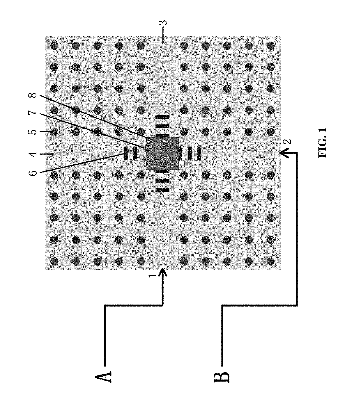
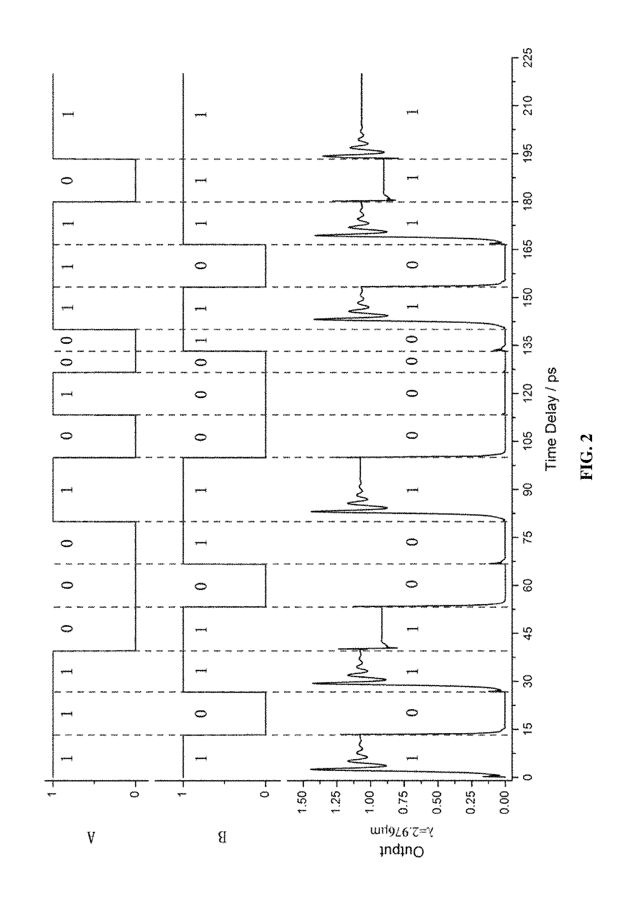
[0036]For the lattice constant d of 1 μm and the operating wavelength of 2.976 μm, the circular high-refractive-index linear-dielectric pillar 5 has the radius of 0.18 μm; the first rectangular high-refractive-index linear-dielectric pillar 6 has the long sides of 0.613 μm and short sides of 0.162 μm; the second rectangular high-refractive-index linear-dielectric pillar 7 is as large as the first rectangular high-refractive-index linear-dielectric pillar 6; the central nonlinear-dielectric pillar 8 has the side length of 1.5 μm, and the third-order nonlinear coefficient of 1.33×10⁻² μm2 / V2; and the distance between every two adjacent rectangular linear-dielectric pillar s is 0.2668 μm.

[0037]Referring to the 2D PhC cross-waveguide nonlinear cavity shown in FIG. 1, a signal A is input to the first input port 1, and a signal B is input to the second input port 2.

[0038]For the 2D PhC nonlinear cavity shown in FIG. 1 in the present invention and for the signal wave forms A and B, which a...

embodiment 2

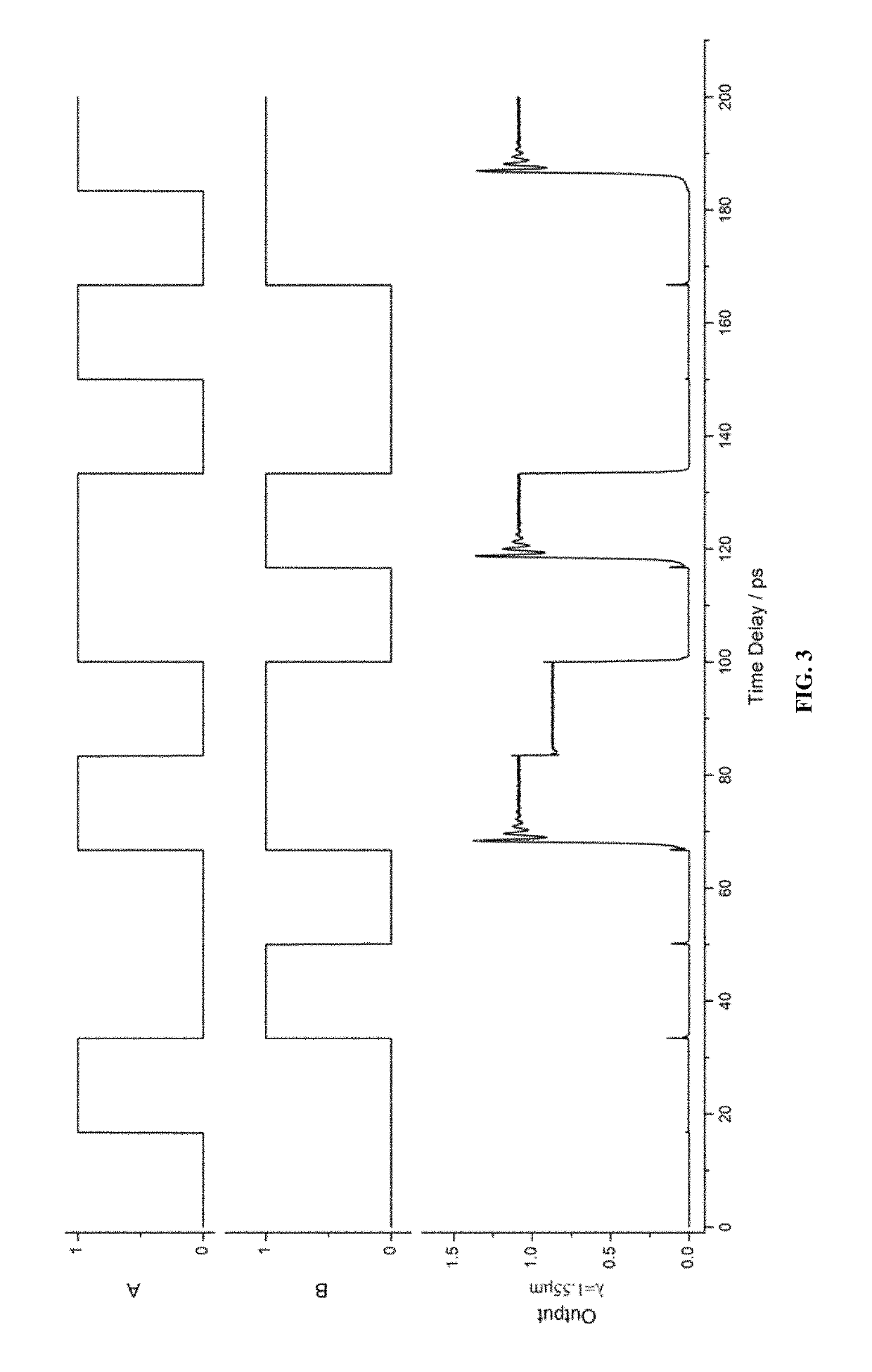
[0046]when the lattice constant d is 0.5208 μm and the operating wavelength is 1.55 μm, the circular high-refractive-index linear-dielectric pillar 5 has the radius of 0.093744 μm; the first rectangular high-refractive-index linear-dielectric pillar 6 has the long sides of 0.3192504 μm and short sides of 0.0843696 μm; the second rectangular high-refractive-index ear-dielectric pillar 7 is as large as the first rectangular high-refractive-index linear-dielectric pillar 6; the central nonlinear-dielectric pillar 8 has the side length of 0.7812 μm and the third-order nonlinear coefficient of 1.33×10⁻² μm2 / V2; and the distance between every two adjacent rectangular linear-dielectric pillars is 0.13894944 μm.

[0047]Based on the above dimension parameters, for a signal A and a signal B with the waveforms shown in FIG. 3 are respectively input to the first input port 1 and the second input port 2, output waveform diagrams at the lower part of FIG. 3 can be obtained. It can be known from the...


PUM

PropertyMeasurementUnit
dielectric constantaaaaaaaaaa
refractive indexaaaaaaaaaa

Abstract

The present invention discloses a photonic crystal memory type all-optical “AOR” logic gate, and including photonic crystal structure; the photonic crystal structure includes two input ports, an output port and an idle port; a first input end and a second input end of the photonic crystal structure are respectively connected with a signal A and a signal B. The present invention has the advantages in high contrast of high and low logic output, high in computing speed, strong in anti-interference capability, and ease of integration with other optical logic elements.

Description

CROSS-REFERENCE TO RELATED APPLICATION[0001]This application is a continuation application of PCT Application No. PCT / CN2015 / 097844 filed on Dec. 18, 2015, which claims priority to Chinese Patent Application No. 201410799755.2 filed on Dec. 19, 2014, the entire contents of which are hereby incorporated by reference.FIELD OF THE INVENTION[0002]The present invention relates to a two-dimensional (2D) photonic crystal (PhC) and optical “AOR” logic gate.BACKGROUND OF THE INVENTION[0003]In 1987, the concept of PhC was proposed separately by E. Yablonovitch from United States Bell Labs who discussed how to suppress spontaneous radiation and by S. John from Princeton University who made discussions about photonic localization. A PhC is a material structure in which dielectric materials are arranged periodically in space, and is usually an artificial crystal including of two or more materials having different dielectric constants.[0004]With the emergence of and in-depth search on PhC, people...

Claims


Application Information

Patent Timeline
Patent Type & Authority Patents(United States)
IPC IPC(8): G02F1/365G02F3/00G02B6/122G02B6/125B82Y20/00G02B6/12
CPCG02F1/365G02F3/00G02B6/125G02B6/1225G02B2006/1213B82Y20/00G02F2202/32G02F1/3501
Inventor OUYANG, ZHENGBIAOYU, QUANQIANG
Owner SHENZHEN UNIV
Features
  • R&D
  • Intellectual Property
  • Life Sciences
  • Materials
  • Tech Scout
  • Unparalleled Data Quality
  • Higher Quality Content
  • 60% Fewer Hallucinations
Learn More