Organic thin-film laminate and organic electroluminescence element

a technology of organic electroluminescent elements and thin films, applied in the field of organic thin films and organic electroluminescent elements, can solve the problems of large scale of curing treatment devices and damage, and achieve the effects of reducing performance deterioration, smallest atomic radius, and largest electro negativity valu

Active Publication Date: 2020-01-07
KONICA MINOLTA INC +1
View PDF17 Cites 0 Cited by
  • Summary
  • Abstract
  • Description
  • Claims
  • Application Information

AI Technical Summary

Benefits of technology

[0023]The present invention enables to provide an organic thin-film laminate capable of suppressing performance deterioration even when an intermediate layer is formed using a wet method, and the present invention enables to provide an organic electroluminescent element provided with the organic thin-film laminate.
[0024]An expression mechanism or an action mechanism of the effects of the present invention is not clearly identified, but it is supposed as follows.
[0025]The fluorinated solvent included in the present invention has the following feature. A fluorine atom has a largest electro negativity value among all of the elements, and it has a smallest atomic radius among halogen atoms. Therefore, in spite of the fact that a C—F bond has a large polarity, the C—F bond has a small distance and the C—F bond has a small polarizability. The small polarizability of the C—F bond means that it has a weak intermolecular force and it results in having a small surface free energy. By this, the fluorinated solvent will produce an excellent water repellent and oil repellent property and a non-adhesive property. It is possible to suppress dissolution of the material used for the underlayer, Further, it is possible to suppress performance deterioration caused by aggregation of the dissolved transport materials or it is possible to suppress penetration to the underlayer.
[0026]According to the present invention, the intermediated is formed with a conductive polymer having no polymerizable group and a fluorinated solvent. As a result, it is possible to coat a conductive polymer having no polymerizable group by dissolving in a polar solvent, and at the same time, it is possible to suppress dissolving of the underlayer material. Thus, it is possible to strike a balance between the two which seem incompatible.

Problems solved by technology

When an upper layer is formed in a position remoted from the adjacent position of an underlayer, a solvent used for the upper layer will penetrate in the underlayer to result in causing a problem of making damage.
However, an organic thin-film laminate or a substrate may cause damage, and a curing treatment device may be a large scale.

Method used


Image

  • Organic thin-film laminate and organic electroluminescence element
  • Organic thin-film laminate and organic electroluminescence element
  • Organic thin-film laminate and organic electroluminescence element

Examples


example 1

101>>

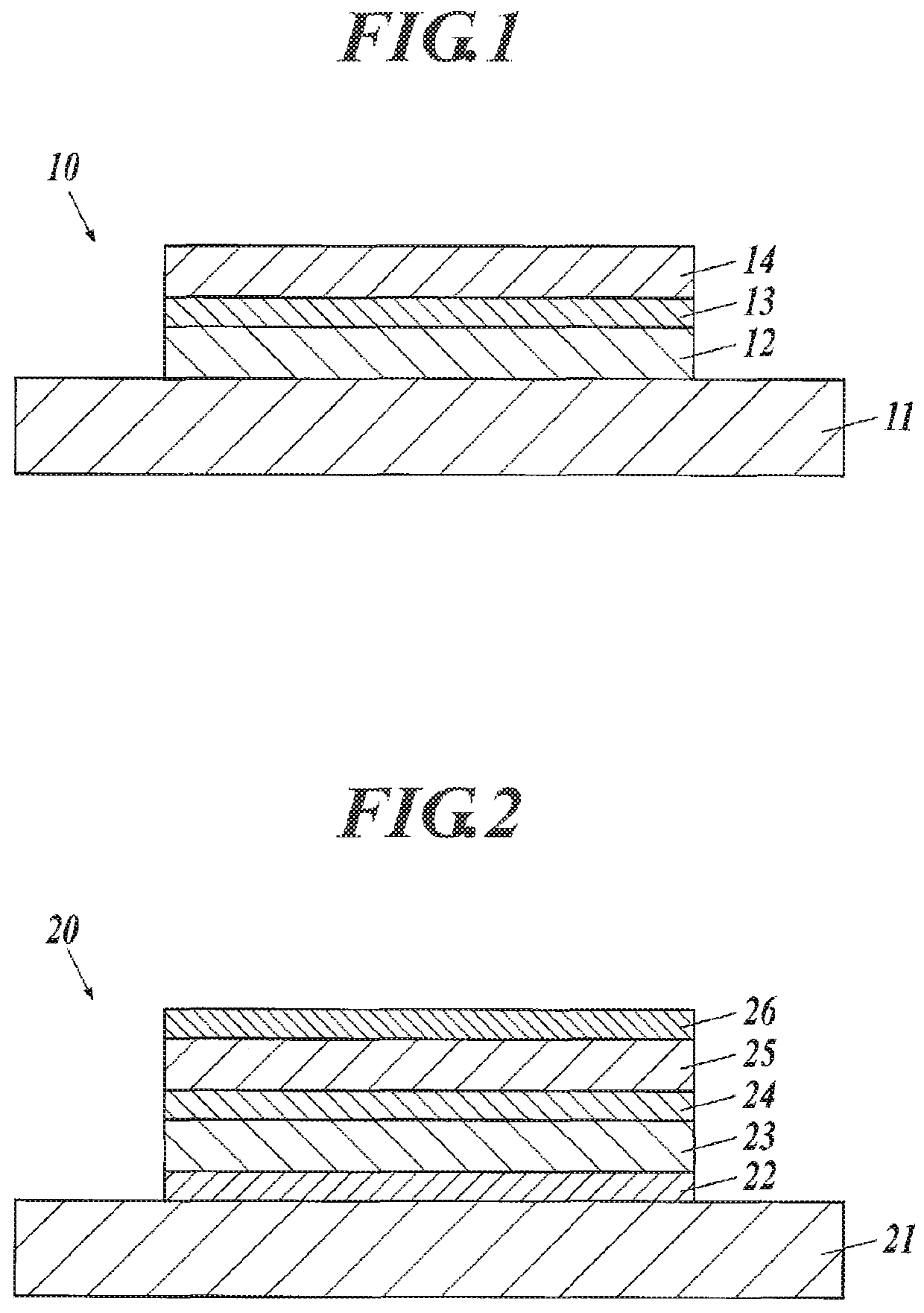
[0180]A first light emitting layer, an intermediate layer and a second light emitting layer were formed on a substrate, then it was sealed as described in the following. Thus, it was obtained an organic thin-film laminate 101 having a light emitting area of 5 cm×5 cm.

(Preparation of Substrate)

[0181]An inorganic gas barrier film made of SiOx with a layer thickness of 500 nm was formed on the total surface of polyethylene naphthalate (made by Teijin-DuPont Co. Ltd., hereafter, it is abbreviated as PEN) to which a first light emitting layer was formed by using an atmospheric pressure plasma discharge processor having a structure described in JP-A No. 2004-68143. By this it was formed a flexible substrate having a gas barrier property of an oxygen permeability of 0.001 mL / m2 / day or less, and a water vapor permeability 1 of 0.001 g / m2 / day or less.

(Formation of First Electrode Layer)

[0182]ITO (indium tin oxide) was sputtered on the above-described substrate to form a film having a th...

example 2

201>>

[0228]A bottom emission type organic EL element having the following constitution was formed. On an substrate were formed with: an anode / a first light emitting unit (a hole injection layer / a hole transport layer / a first light emitting layer) / intermediate layers (a first intermediate layer / a second intermediate layer / a third intermediate layer) / a second light emitting unit (a hole transport layer / a second light emitting layer / an electron transport layer / an electron injection layer) / a cathode. This was sealed to obtain an organic thin-film laminate 201.

(Preparation of Substrate)

[0229]An inorganic gas barrier film made of SiOx with a layer thickness of 500 nm was formed on the total surface of polyethylene naphthalate (made by Teijin-DuPont Co. Ltd., hereafter, it is abbreviated as PEN) to which an anode was formed by using an atmospheric pressure plasma discharge processor having a structure described in JP-A No. 2004-68143.

[0230]By this it was formed a flexible substrate having ...

example 3

[0299]An organic EL element 301 that emits white light was produced in the same manner as production of the organic EL element 201 in Example 2 except that the forming methods of the second light emitting layer, the electron transport layer, and the electron injection layer in the second light emitting unit were changed as described in the following.

(Formation of Second Light Emitting Unit—Second Light Emitting Layer)

[0300]On the third intermediate layer was formed a hole transport layer for the second light emitting unit having the same constitution as the first light emitting unit in the same manner as formation of the organic EL element 201. Thereon was formed a second light emitting layer material having the following composition with a die coat method at a rate of 5 m / min. After natural drying, the coated substance was kept at 120° C. for 30 minutes. Thus it was formed a second light emitting layer having a thickness of 40 nm.

[0301]

Host compound S-26:9.5mass partsPhosphorescent...


PUM

PropertyMeasurementUnit
solubilityaaaaaaaaaa
dielectric constantaaaaaaaaaa
thicknessaaaaaaaaaa

Abstract

An object of the present invention is to provide an organic thin-film laminate capable of suppressing function reduction even when an intermediate layer is formed using a wet method. The organic thin-film laminate has one or more organic functional layers, the organic thin-film laminate being characterized by being provided with: a first light-emitting layer 12 containing a first light-emitting-layer material that is soluble in a polar solvent other than a fluorinated solvent, and is insoluble in a fluorinated solvent; a second light-emitting layer 14 laminated on the first light-emitting layer 12; and one or more intermediate layers comprising a non-curable material, the intermediate layers being provided between the first light-emitting layer 12 and the second light-emitting layer 14, an intermediate layer 13, among the one or more intermediate layers, containing a conductive polymer having no polymerizable group and containing a fluorinated solvent in the range of 1-1000 mass ppm.

Description

CROSS REFERENCE TO RELATED APPLICATION[0001]This Application is a 371 of PCT / JP2016 / 058807 filed on Mar. 18, 2016, which, in turn, claimed the priority of Japanese Patent Application No. JP 2015-141031 filed on Jul. 15, 2015, both applications are incorporated herein by reference.TECHNICAL FIELD[0002]The present invention relates to an organic thin-film laminate and an organic electroluminescent element. In particular, the present invention relates to an organic thin-film laminate capable of suppressing performance deterioration even when an intermediate layer is formed using a wet method, and the present invention relates to an organic electroluminescent element provided with the organic thin-film laminate.BACKGROUND[0003]In the past, an organic electroluminescent element (hereafter, it is also called as an organic EL element) has been cited as an emission-type electronic display device.[0004]An organic electroluminescent element has a constitution in which a light emitting layer c...

Claims


Application Information

Patent Timeline
Patent Type & Authority Patents(United States)
IPC IPC(8): H01L51/52C09K11/06H01L51/00H01L51/50
CPCH01L51/5278H01L51/004H01L51/5012C09K11/06H01L51/5016H01L51/0067H01L51/0085H01L51/0039C09K2211/1014C09K2211/1029H01L51/0083H01L51/0059C09K2211/1011C09K2211/185H01L2251/303H01L51/0058H01L51/006H01L51/0056H01L51/0072H01L51/0073Y10T428/1036H01L51/0054C09K2211/1007C09K2211/1044Y10T428/10H05B33/14H05B33/26H10K71/15H10K85/10H10K85/115H10K85/631H10K85/331H10K85/654H10K85/6574H10K85/342H10K50/115H10K85/6572H10K50/131C07D405/14C07D519/00H10K50/84H10K71/00C09K2323/00C09K2323/03H10K50/19H10K50/11H10K85/141H10K85/622H10K85/624H10K85/626H10K85/633H10K2101/10H10K2102/00
Inventor OIKAWA, KAZUHIROIWASAKI, TOSHIHIKOCHIBA, TAKAYUKIPU, YONG-JINKIDO, JUNJI
Owner KONICA MINOLTA INC
Why Eureka
Try Eureka