Method of manufacturing emitter

a manufacturing method and technology of emitters, applied in the manufacture of electrode systems, electric discharge tubes/lamps, discharge tube coatings, etc., can solve the problems of degrading processing precision, difficult to form the tip in a pyramid shape, and difficult to perform a process

Active Publication Date: 2020-05-19
HITACHI HIGH TECH SCI CORP
View PDF5 Cites 1 Cited by
  • Summary
  • Abstract
  • Description
  • Claims
  • Application Information

AI Technical Summary

Benefits of technology

[0022]According to the present invention, it is possible to provide a method of manufacturing an emitter in which the tip of the emitter can be formed into a desired shape even when various materials are used for the emitter.

Problems solved by technology

However, there are some emitter materials in which it is difficult to form the tip in a pyramid shape through the electrolytic polishing.
There is a likelihood that this trace may degrade the precision of processing when the distal tip of the emitter material is sharpened to an atomic level, and also there is a likelihood of making it difficult to perform a process performed after etching process during the processing of the emitter material.
As a result, the yield in the processing of the emitter material may be deteriorated, and the trace may adversely affect the stable operation of the ion current when used after emitter processing or the regeneration of a structure of the distal tip.

Method used


Image

  • Method of manufacturing emitter
  • Method of manufacturing emitter
  • Method of manufacturing emitter

Examples


embodiment

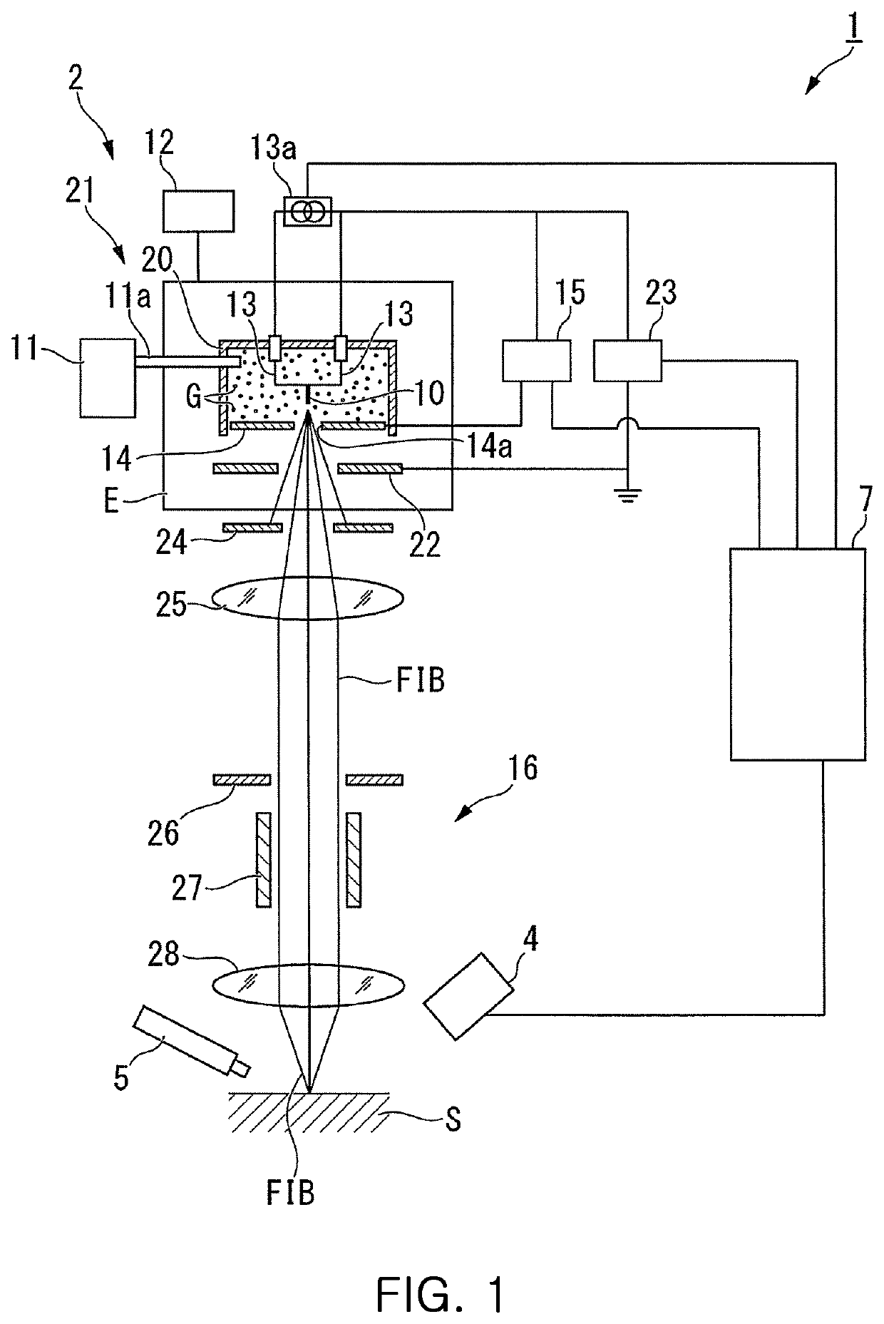
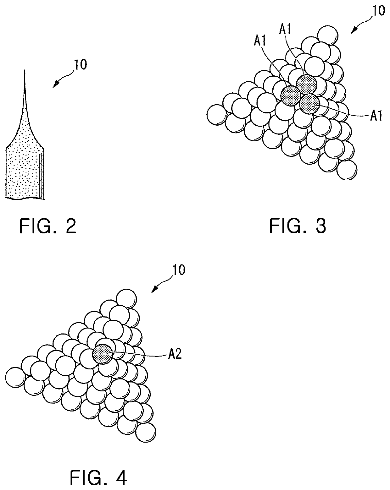
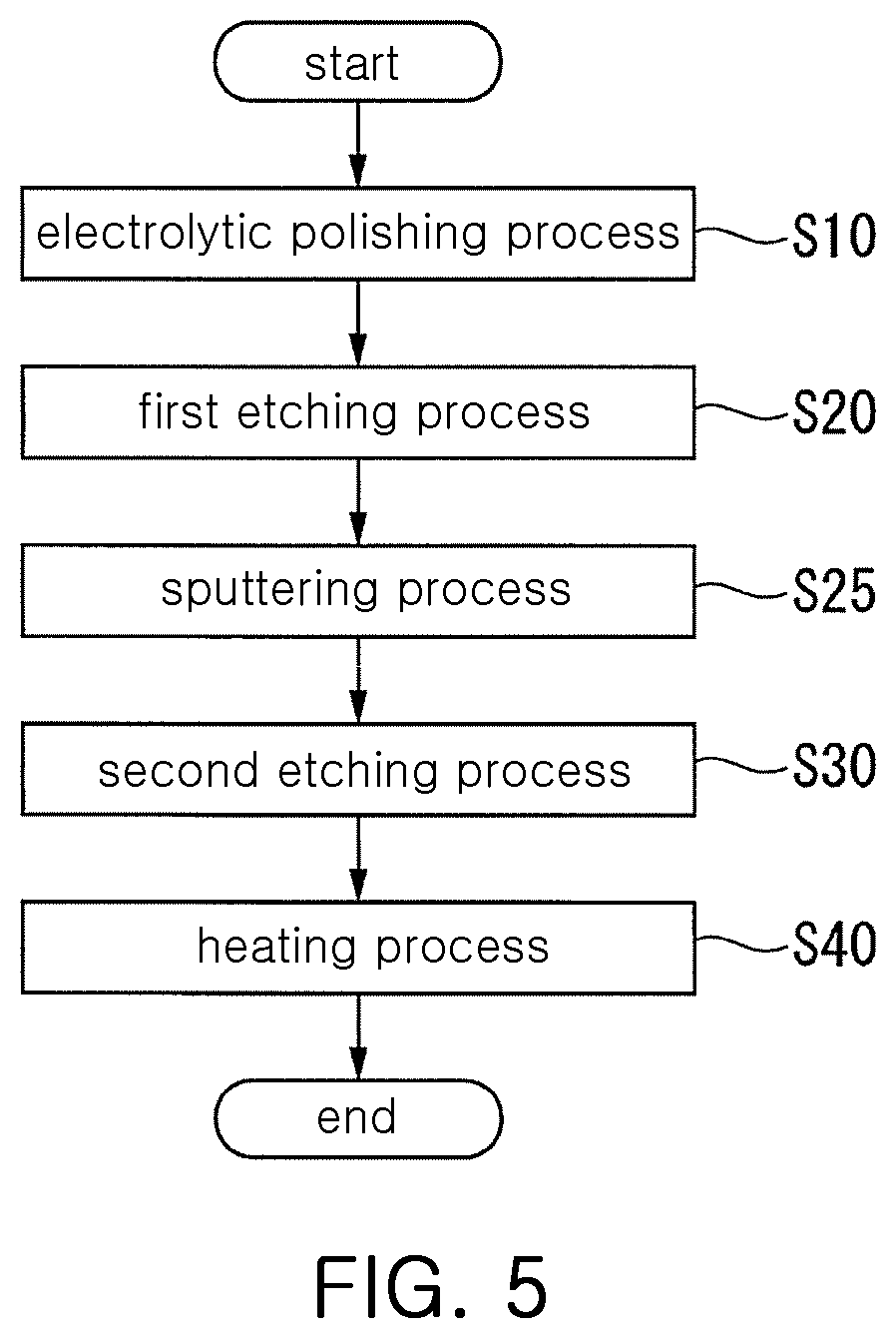
[0040]Hereinafter, an embodiment of the present invention will be described with reference to the drawings. Further, according to an embodiment, an emitter constituting a gas field ion source (GFIS) and used as an emission source of ion beam is described as an example.

[0041]First, with reference to FIG. 1, a configuration of a focused ion beam apparatus having a focused ion beam column having the gas field ion source will be described. The focused ion beam apparatus 1 shown in FIG. 1 is an example of a focused ion beam apparatus having the focused ion beam column having the gas field ion source.

[0042]

[0043]As shown in FIG. 1, the focused ion beam apparatus 1 includes a focused ion beam column 2 for irradiating a sample S placed on a stage (not shown) with a focused ion beam FIB, a detector 4 for detecting secondary charged particles generated by emitting the focused ion beam FIB, a gas gun 5 for supplying a source gas used to form a deposition film, and a control unit 7 for displayi...


PUM

PropertyMeasurementUnit
diameteraaaaaaaaaa
sizeaaaaaaaaaa
apex angle θ1aaaaaaaaaa

Abstract

Disclosed is a method of manufacturing an emitter in which the tip of the emitter can be formed into a desired shape even when various materials are used for the emitter. The method includes performing an electrolytic polishing process of polishing a front end of a conductive emitter material so that a diameter of the front end is gradually reduced toward a tip; performing a first etching process by irradiating a processing portion of the emitter material processed by the electrolytic polishing process with a charged particle beam; performing a sputtering process by irradiating the pointed portion formed by the first etching process with a focused ion beam; and performing a secondary etching process of further sharpening the tip by an electric field induced gas etching processing while observing a crystal structure of the tip of the pointed portion processed by the sputtering process using a field ion microscope.

Description

CROSS REFERENCE TO RELATED APPLICATION(S)[0001]This application claims the benefit of Japan Patent Application No. JP 2018-030577 filed Feb. 23, 2018, which is hereby incorporated by reference in its entirety into this application.BACKGROUND OF THE INVENTION1. Technical Field[0002]The present invention relates to a method of manufacturing an emitter used as an emission source that emits electrons, ions, and the like.2. Description of the Related Art[0003]In the related art, a focused ion beam apparatus has an ion source for generating ions, and emits a focused ion beam in which ions generated from the ion source are focused. For example, a focused ion beam apparatus having a field ionization type ion source as an ion source is known (see, for example, Patent Document 1).[0004]The field ionization type ion source includes an emitter whose tip is sharpened at an atomic level, a gas source for supplying gas such as nitrogen gas or helium gas to the periphery of the emitter, a cooling u...

Claims


Application Information

Patent Timeline
Patent Type & Authority Patents(United States)
IPC IPC(8): H01J9/02C25F3/16H01J37/305C25F3/08C25F3/00C25F3/26
CPCH01J9/025C25F3/26C25F3/08H01J37/3053C25F3/00C25F3/16H01J2209/012H01J1/3042
Inventor NAKAJIMA, YOKOKAWANAMI, YOSHIMIMORITANI, HIRONORIOBA, HIROSHI
Owner HITACHI HIGH TECH SCI CORP
Why Eureka
Try Eureka