
Carbon nanotube-based thermal interface materials and methods of making and using thereof

a technology of thermal interface materials and carbon nanotubes, which is applied in the direction of lighting and heating apparatus, modifications by conduction heat transfer, and semiconductor/solid-state device details, etc. it can solve the problems of high contact area at such interfaces between surfaces, early termination of tube growth, and difficulty in growing very long cnts on metal substrates. achieve high degree of complian

Active Publication Date: 2020-09-29
CARBICE CORP
View PDF82 Cites 1 Cited by
  • Summary
  • Abstract
  • Description
  • Claims
  • Application Information

AI Technical Summary

Benefits of technology

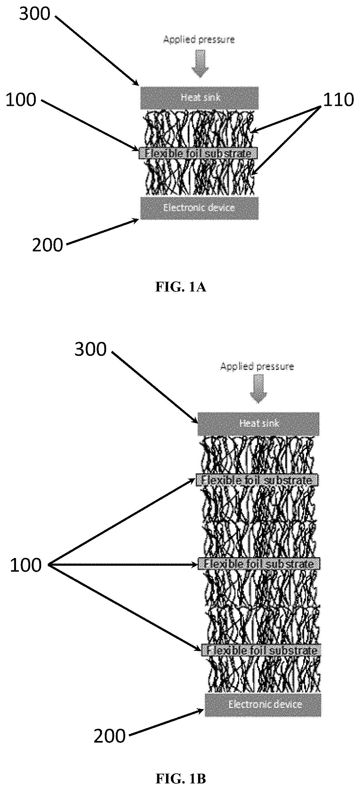
[0010]Two or more CNT arrays are typically stacked to form multilayered or multitiered structures. Stacking of multiple CNT arrays, such that the nanostructure elements from opposing arrays form into tiers in the stack and become at least partially interdigitated with one another. Unlike the stacking of a traditional material, stacked arrays of vertically aligned nanostructures do no suffer from a linear (or worse) increase in thermal resistance with increasing thickness. Accordingly, the resulting multilayered structures can mitigate the adverse impact of thickness and boundaries on energy transport as a result of the interdigitation of the nanostructure elements (i.e., CNTs) of the two or more arrays when contacted. In contrast, for a typical material the resistance to heat transfer is directly proportional to the material's thickness, with an additional interfacial resistance at the interfaces of a multilayered structure.
[0011]For multilayered or multitiered structures formed by stacking of vertically aligned nanostructure materials of CNT arrays, wherein the CNTs of the arrays at least partially interdigitate within or into one another, effectively increasing the density of the CNTs. Typically, the density of CNTs grown on metal substrates is only about 1% of the total volume. When two adjacent layers of CNT arrays are stacked, for example, the density of heat conducting elements, such as CNTs or structures formed thereof, is effectively doubled. As such the resistance to heat transfer per unit length is reduced in kind.
[0012]An advantage of the multilayered or multitiered structures formed by stacking of two or more CNT arrays over traditional bulk materials comes at the interface of the arrays. For example, resistance to heat transfer increases not only due to the increase in thickness of a multilayer stack, but also due to the interfacial resistances between the tiers. Accordingly, between any two adjacent tiers, the boundary between the two tiers is the location of poor heat transfer, relative to the bulk material due to poor contact between the tiers, as well as due to scattering of energy carriers (e.g. electrons or phonons) at the boundary. When interdigitated, the high aspect ratio of the nanostructures, such as CNTs, results in a very high contact area between the tiers minimizing the poor contact area contribution to the inter tier interfacial resistance. Although Kapitza (scattering) resistance cannot be completely eliminated the resistance can be reduced by applying, infiltrating, or backfilling the array or sheet with a polymer, wax, or other secondary material that facilitates thermal / energy transport across the boundary. This transport facilitation may be through the formation of a covalent or weak atomic interaction between the CNT and a secondary material, reduction of acoustic phononic transport mismatch relative to air, or other types of mechanisms.
[0018]In some embodiments the polymer, wax, liquid metal, or other suitable material can reduce the transport resistance between the multiple layers or tiers formed, resulting from improved contact area, a reduction in scattering, or other related mechanisms. In yet other embodiment the tiers formed by stacking of arrays may be bonded by use of an adhesive or a phase-change material.
[0019]CNT arrays and the multilayered or multitiered structures formed by stacking of such CNT arrays exhibit both high thermal conductance and mechanical durability. The multilayered or multitiered structures formed by stacking of CNT arrays described herein can be used as thermal interface materials (TIMs). Accordingly, such materials are well suited for applications where repeated cycling is required. For example, they can be employed as thermal interface materials during ‘burn-in’ testing of electrical components, such as chips. In some embodiments, the inert support / substrate is a surface of a conventional metal heat sink or spreader. This functionalized heat sink or spreader may then be abutted or adhered to a heat source, such as an integrated circuit package. Such TIM materials can also be placed or affixed in between a heat source and a heat sink or heat spreader, such as between an integrated circuit package and a finned heat exchanger, to improve the transfer of heat from the heat source to the heat sink or spreader.

Problems solved by technology

Furthermore, the favorable deformation mechanics of CNTs allow them to efficiently conform to the asperities of adjoining surfaces, resulting in high contact areas at such interfaces between surfaces.
A key challenge, however, in CNT-based TIMs comes from the difficulty in growing very long CNTs on metal substrates.
Unlike CNTs grown on silicon or other inert substrates, the catalyst required for CNT growth suffers from subsurface diffusion when grown on metal substrates, resulting in early termination of tube growth.
Furthermore, defects tend to accumulate in CNTs as their height increases, resulting in CNT arrays with conductivities significantly lower than the 3,000 W / m-K limit otherwise achievable with pristine tubes.

Method used


Image

  • Carbon nanotube-based thermal interface materials and methods of making and using thereof
  • Carbon nanotube-based thermal interface materials and methods of making and using thereof
  • Carbon nanotube-based thermal interface materials and methods of making and using thereof

Examples


example 1

red / Multitiered CNT-Based Thermal Interface Materials (TIMs)

[0137]Methods:

Thermal Measurement System Design

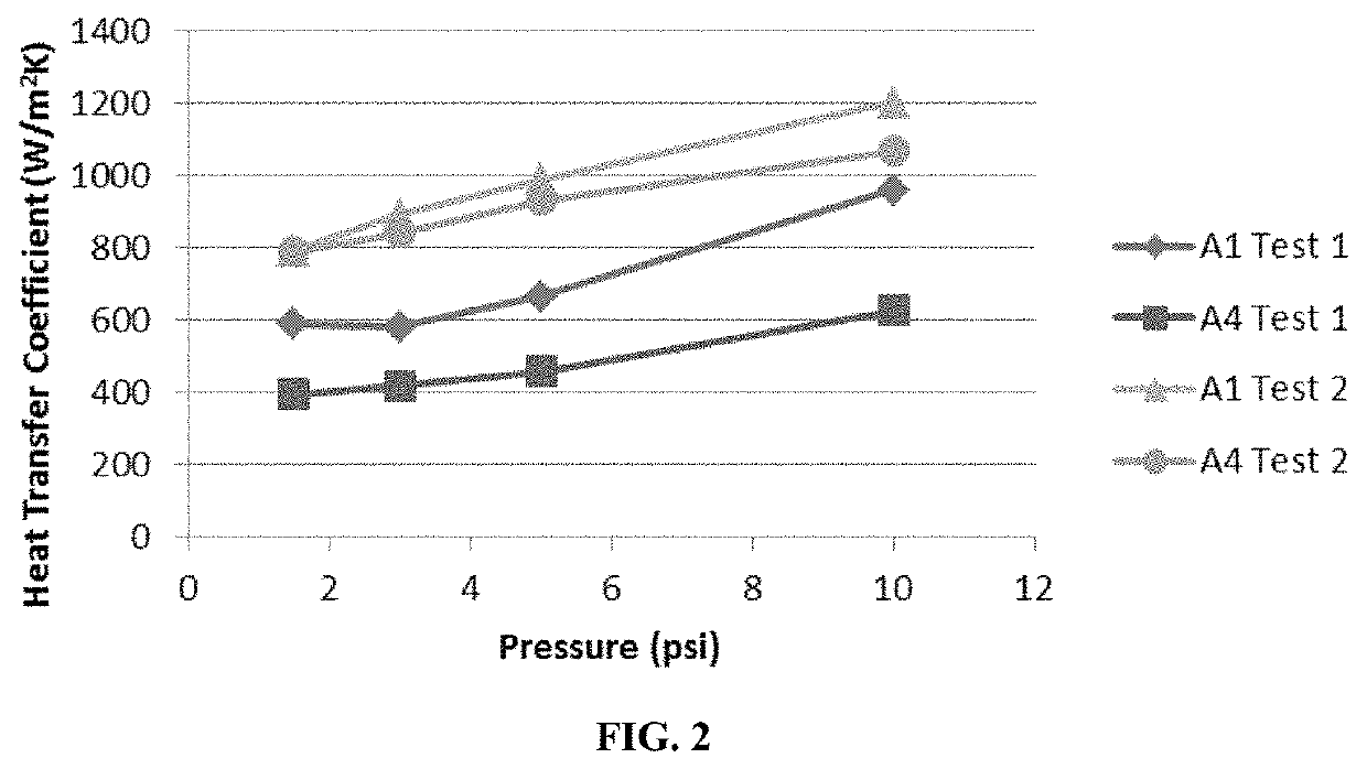
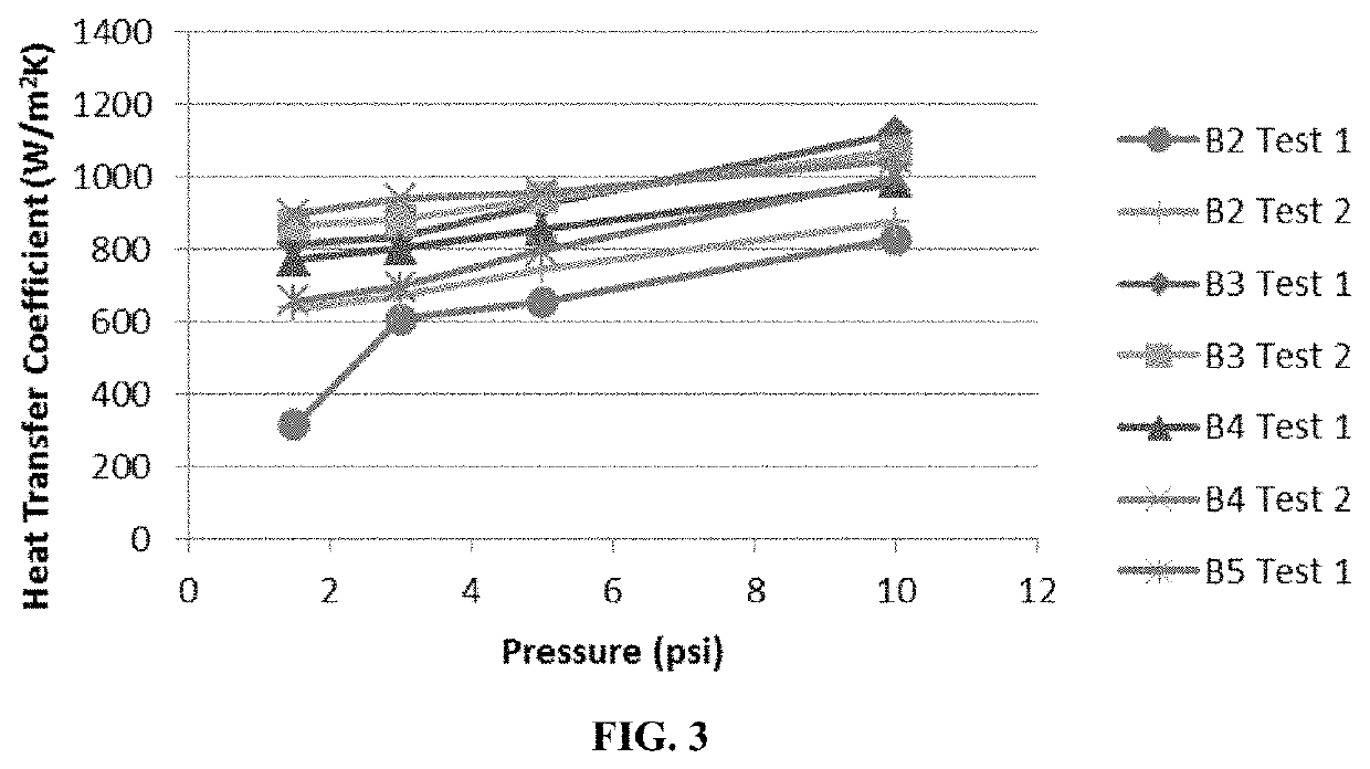
[0138]Heat transfer properties for all test specimens were evaluated using a test fixture (not shown) designed and built based on the methods described in ASTM D5470 “Standard Test Method for Thermal Transmission Properties of Thermally Conductive Electrical Insulation Materials.” It not only allows for deformation of the test specimens but also incorporates a vacuum chamber to minimize conductive and convective heat losses. The vacuum chamber was constructed of stainless steel with an acrylic door, and is capable of maintaining vacuum in the 10−5 torr range. The vacuum chamber sits on the reaction plate of a 1000 lb load frame, with all feedthroughs near the top of the chamber. Thermocouples were fed via a pair of Omega 4-pair feedthroughs (8 thermocouples possible). The cooling tubes possess bulkhead fittings with o-ring seals. The power for the heaters were controlled via a ...

example 2

red / Multitiered CNT-Based Thermal Interface Materials (TIMs) Containing Polymer or Adhesive

[0158]CNT arrays were grown to nominally 100 μm thickness and fully infiltrated with a soft polyurethane polymer. The thermal resistance of each individual pad was measured using a modified ASTM D570 stepped bar apparatus.

[0159]The individual samples were stacked using various methods, and the thermal resistance of the resulting stack was measured in the same manner as the single tiers.

[0160]First, two individual array samples with measured thermal resistances of 1.37 and 1.5 cm2-K / W respectively were stacked on top of one another. Solvent known to dissolve the polymer that was used to infiltrate the array was placed between the stacks to place the interface in a liquid state. The resulting stack was allowed to dry under pressure until the solvent was fully evaporated. The stack was then measured in the stepped bar system with a resulting resistance of 1.5 cm2-K / W. In this example, the thickne...

example 3

red / Multitiered CNT-Based Thermal Interface Materials (TIMs)

[0162]Sample Fabrication:

[0163]Vertically aligned carbon nanotube (CNT) arrays were grown on aluminum foil as the base substrate. Both sides of 50 μm thick aluminum foil were coated with an iron catalyst layer and the CNTs were grown via low pressure chemical vapor deposition with acetylene and hydrogen as precursor gases and growth being performed at 630° C. in order to stay below the melting temperature of the Al substrate. CNTs were grown to 7-10 μm on both sides of the substrate with an 8 minute growth time. One-tier CNT-based thermal interface material (non-stacked) and two- and four-tiered (formed by stacking two or four double-sided CNT arrays) CNT-based thermal interface materials (TIMs) having an area of 1 cm×1 cm were prepared for testing.

[0164]Testing Methods:

[0165]In order to measure the thickness, compression, and rebound of the one and three-tiered TIMs prepared, a Precision Thickness Gauge—FT3V by Hanatek® In...


PUM

PropertyMeasurementUnit
temperatureaaaaaaaaaa
pressuresaaaaaaaaaa
pressuresaaaaaaaaaa

Abstract

Multilayered or multitiered structures formed by stacking of vertically aligned carbon nanotube (CNT) arrays and methods of making and using thereof are described herein. Such multilayered or multitiered structures can be used as thermal interface materials (TIMs).

Description

CROSS REFERENCE TO RELATED APPLICATIONS[0001]This application claims priority to and benefit of U.S. Ser. No. 62 / 343,458, filed May 31, 2016, which is hereby incorporated herein by reference in its entity.FIELD OF THE INVENTION[0002]This invention is in the field of carbon nanotube arrays or sheets, particularly arrays or sheets which are stacked to form multilayered or multitiered structures and methods of making and using thereof.BACKGROUND OF THE INVENTION[0003]Carbon nanotube (CNT) arrays are an attractive solution for enhancing thermal transport between surfaces. CNTs can be grown on metal substrates, eliminating concerns associated with pump out or voiding that liquid thermal interface materials (TIMs) and greases may suffer from.[0004]The high in-plane conductivity of individual nanotubes (as high as 3,000 W / m-K) means that even at relatively low CNT densities (typical CNT fill factors are on the order of 1%) the cross plane thermal conductance of a CNT-based TIM can be compe...

Claims


Application Information

Patent Timeline
Patent Type & Authority Patents(United States)
IPC IPC(8): F28F7/00H05K7/20H01L23/373H01L23/42C01B32/16C23C14/06
CPCH01L23/373H05K7/20481H01L23/3735H01L23/42C01B32/16C23C14/06C01B2202/24B82B3/0014B82Y30/00B82Y40/00C09K5/14H05K7/2039H05K9/0081B32B37/26B32B7/10B32B9/007B32B37/10B32B37/12B32B7/12C09J2301/302B32B2037/243B32B2309/12
Inventor COLA, BARATUNDEPRINZI, LEONARDOGREEN, CRAIG
Owner CARBICE CORP
Learn More